Table 2. serial data format, Pic16 with ssp module and pic17 interface – Rainbow Electronics MAX5123 User Manual
Page 13
MAX5122/MAX5123
+5V/+3V, 12-Bit, Serial, Force/Sense DACs
with 10ppm/°C Internal Reference
______________________________________________________________________________________
13
The 16-bit input word may be sent in two 1-byte pack-
ets (SPI-, MICROWIRE-, and PIC16/PIC17-compatible),
with CS low during this period. The control bits C2, C1,
and C0 (table 1) determine:
•
The clock edge on which DOUT transitions,
•
The state of the user-programmable logic output,
•
The configuration of the device after shutdown.
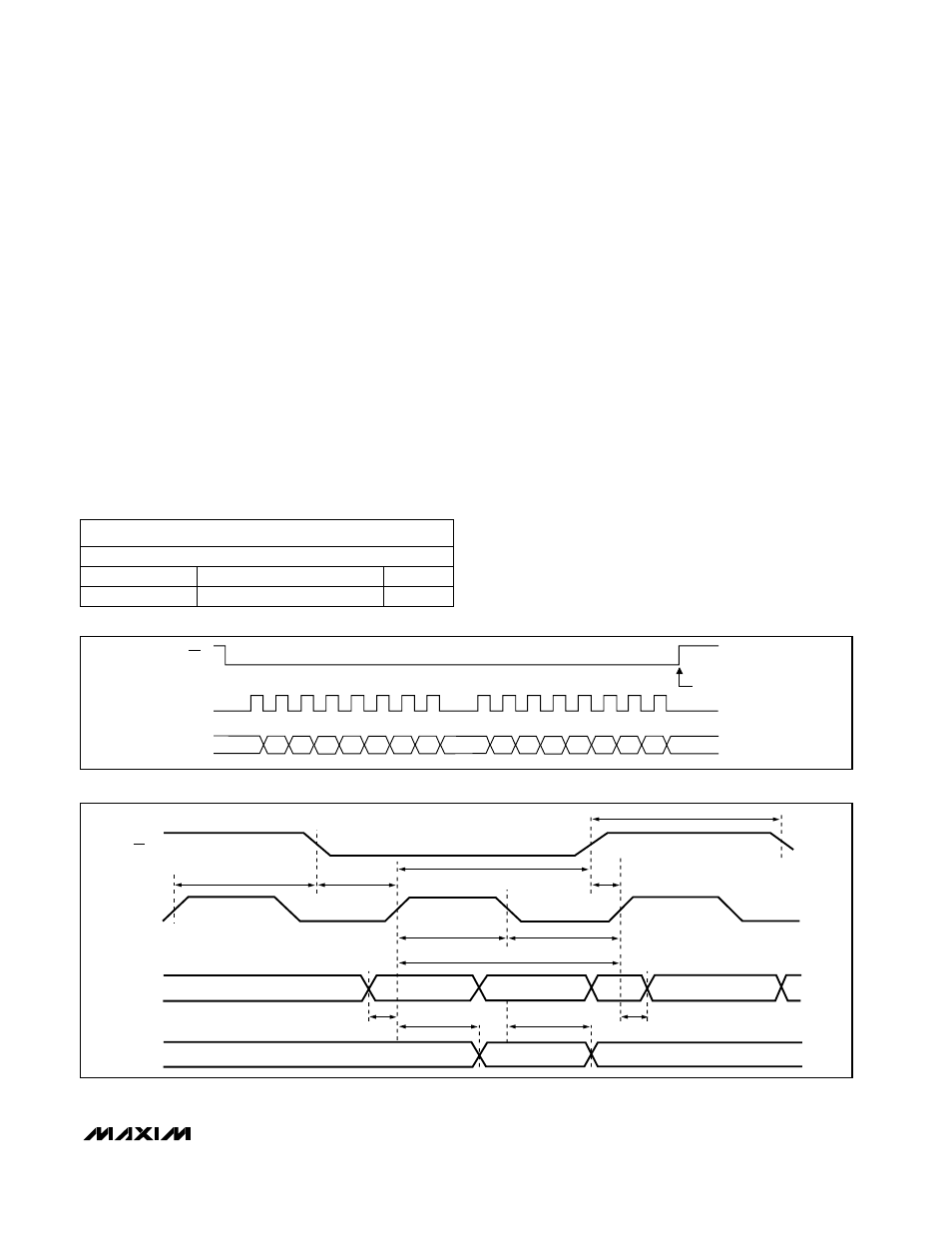
The general timing diagram in Figure 6 illustrates how
data is acquired. CS must be low for the part to receive
data. With CS low, data at DIN is clocked into the regis-
ter on the rising edge of SCLK. When CS transitions
high, data is latched into the input and/or DAC regis-
ters, depending on the setting of the three control bits
C2, C1, and C0. The maximum serial clock frequency
guaranteed for proper operation is 10MHz for the
MAX5122 and 6.6MHz for the MAX5123. Figure 7
depicts a more detailed timing diagram of the serial
interface.
PIC16 with SSP Module
and PIC17 Interface
The MAX5122/MAX5123 are compatible with a
PIC16/PIC17 microcontroller (µC), using the synchro-
nous serial port (SSP) module. To establish SPI commu-
nication, connect the controller as shown in Figure 4
and configure the PIC16/PIC17 as system master by ini-
tializing its synchronous serial port control register (SSP-
CON) and synchronous serial port status register
(SSPSTAT) to the bit patterns shown in Tables 3 and 4.
In SPI mode, the PIC16/PIC17 µCs allow eight bits of
data to be synchronously transmitted and received
simultaneously. Two consecutive 8-bit writings (Figure
6) are necessary to feed the DAC with three control bits,
12 data bits, and one sub-bit. DIN data transitions on
the serial clock’s falling edge and is clocked into the
DAC on SCLK’s rising edge. The first eight bits of DIN
contain the three control bits (C2, C1, C0) and the first
five data bits (D11–D7). The second 8-bit data stream
contains the remaining bits (D6–D0), and the sub-bit S0.
Control Bits
MSB ............................................................................... LSB
D11................................D0
C2, C1, C0
CS
SCLK
DIN
COMMAND
EXECUTED
9
8
16
1
C1
C2
S0
C0
D11 D10
D9
D8
D5
D4
D3
D2
D1
D0
D7
D6
Figure 6. Serial-Interface Timing
SCLK
DIN
DOUT
t
CS0
t
CSS
t
CL
t
CH
t
CP
t
CSW
t
CS1
t
CSH
t
DS
t
DO1
t
DO2
t
DH
CS
Figure 7. Detailed Serial-Interface Timing
Table 2. Serial Data Format
⇐
16 BITS OF SERIAL DATA
⇒
Sub-Bit
S0
MSB ..... Data Bits ..... LSB