Absolute maximum ratings, Electrical characteristics – Rainbow Electronics MAX4995 User Manual
Page 2
MAX4995A/AF/AL/MAX4995B/MAX4995C
50mA to 600mA Programmable
Current-Limit Switches
2
_______________________________________________________________________________________
ABSOLUTE MAXIMUM RATINGS
Stresses beyond those listed under “Absolute Maximum Ratings” may cause permanent damage to the device. These are stress ratings only, and functional
operation of the device at these or any other conditions beyond those indicated in the operational sections of the specifications is not implied. Exposure to
absolute maximum rating conditions for extended periods may affect device reliability.
IN, ON,
ON, FLAG, OUT, and SETI to GND .............-0.3V to +6V
Current into Any Pin (Except IN, OUT)................................20mA
OUT Short Circuit to GND .................................................800mA
Continuous Power Dissipation (T
A
= +70°C) (Note 1)
10-Pin UTQFN (derate 6.99mW/ °C above
T
A
= +70°C) ................................................................559mW
Junction-to-Ambient Thermal Resistance (
θ
JA
)
(Note 2) ...................................................................143.1°C/W
Operating Temperature Range .........................-40°C to +125°C
Storage Temperature Range .............................-65°C to +150°C
Junction Temperature ......................................................+150°C
Lead Temperature (soldering, 10s) .................................+300°C
Note 1: These power limits are defined by the thermal characteristics of the package, maximum function temperature (+150°C), and
the JEDEC51-7 defined setup. Maximum power dissipation could be lower, limited by the thermal-shutdown protection
included in this IC.
Note 2: Package thermal resistances were obtained using the method described in JEDEC specification JESD51-7, using a four-
layer board. For detailed information on package thermal considerations, refer to
www.maxim-ic.com/thermal-tutorial
.
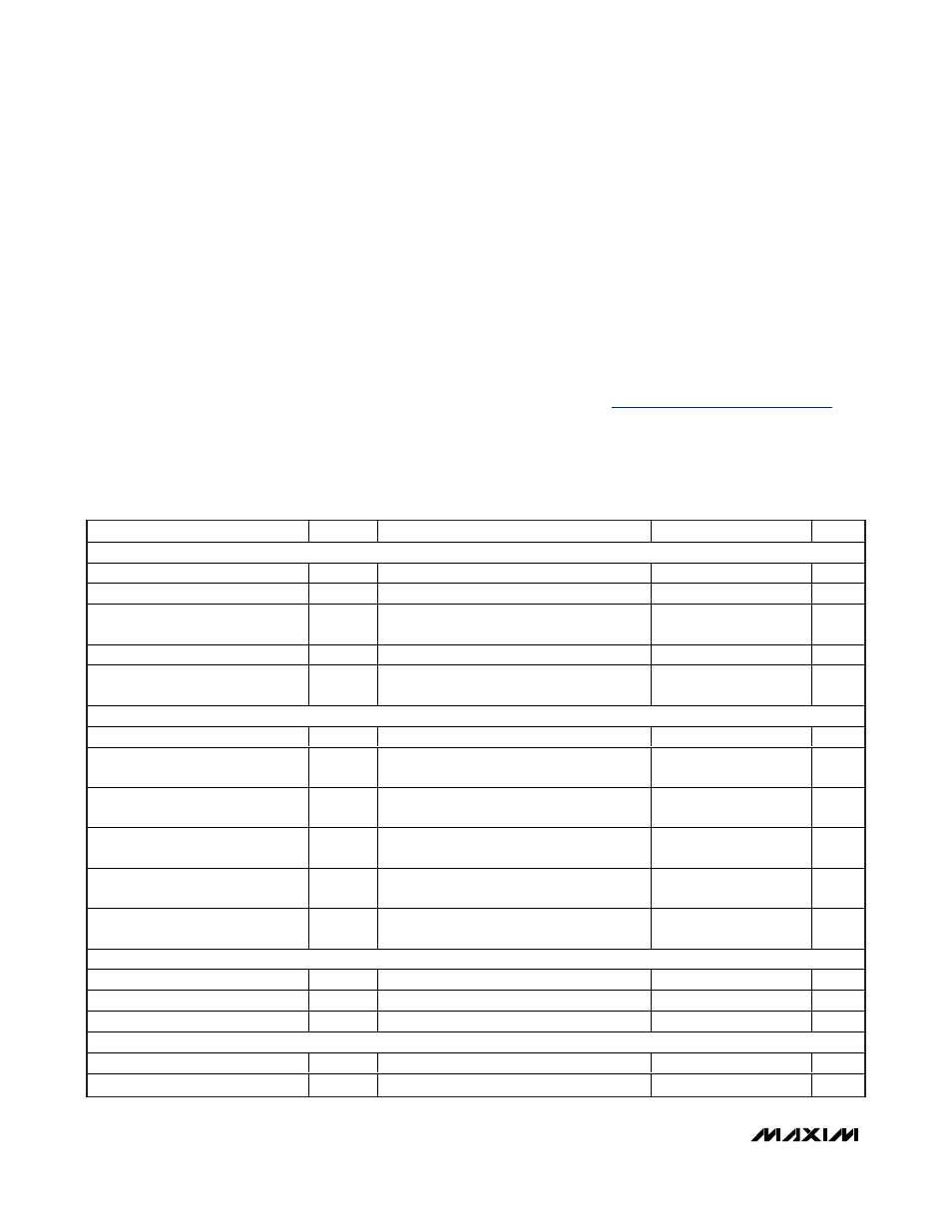
ELECTRICAL CHARACTERISTICS
(V
IN
= +1.7V to +5.5V, R
SETI
= 94.3kΩ, C
IN
= 1µF, and T
A
= T
J
= -40°C to +125°C, unless otherwise noted. Typical values are at V
IN
= +3.3V,
T
A
= +25°C.)
PARAMETER
SYMBOL
CONDITIONS
MIN
TYP
MAX
UNITS
SUPPLY OPERATION
Operating Voltage
V
IN
1.7
5.5
V
Quiescent Current
I
Q
I
OUT
= 0, switch on, V
IN
= 3.3V
170
300
µA
Latchoff Current
I
LATCH
V
IN
= 3.3V, I
OUT
= 0 after an overcurrent
fault (MAX4995B)
8
15
µA
Shutdown Forward Current
I
SHDN
V
ON
= 0, V
ON
= V
IN
, V
IN
= 5.5V, V
OUT
= 0
0.01
5
µA
Shutdown Reverse Current
I
RSHDN
V
ON
= 0, V
ON
= V
IN
, V
IN
= 1.7V,
V
OUT
= 5.5V (current into OUT)
0.01
1
µA
INTERNAL FET
Switch-On Resistance
R
ON
V
IN
= 3.3V, I
OUT
lower than I
LIM
130
350
m
Ω
Normalized Current-Limit Accuracy
I
LIM
= 50mA to 600mA, V
IN
- V
OUT
= 1V,
V
IN
= 3.3V (Note 3)
0.9
1
1.1
—
(R
SETI
+ 2.48) x I
LIM
Product
I
LIM
= 50mA to 600mA, V
IN
- V
OUT
= 1V,
V
IN
= 3.3V
26138
29042
31946
V
Reverse Blocking Current
V
OUT
> V
IN
+ 300mV after reverse-current-
limit shutdown
10
µA
Reverse Blocking Threshold
V
OUT
= V
IN
+ 300mV, OUT falling until switch
turns on
35
110
210
mV
FLAG Assertion Drop Voltage
Threshold
V
FA
Increase (V
IN
- V
OUT
) drop until FLAG
asserts, I
OUT
limiting, V
IN
= 3.3V
650
mV
ON,
ON INPUT
ON, ON Input Leakage
I
LEAK
V
ON
, V
ON
= V
IN
or GND
-1
+1
µA
ON, ON Input Logic-High Voltage
V
IH
1.6
V
ON, ON Input Logic-Low Voltage
V
IL
0.4
V
FLAG OUTPUT
FLAG Output Logic-Low Voltage
I
SINK
= 1mA
0.4
V
FLAG Output Leakage Current
V
IN
= V
FLAG
= 5.5V, FLAG deasserted
1
µA