Chip information – Rainbow Electronics MAX5081 User Manual
Page 15
MAX5080/MAX5081
1A, 40V, MAXPower Step-Down
DC-DC Converters
______________________________________________________________________________________
15
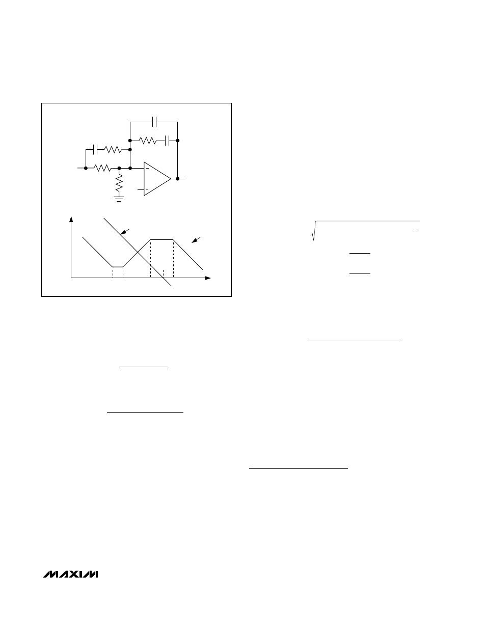
Since R3 >> R6, R3 + R6 can be approximated as R3.
R3 is then calculated as:
f
P3
is set at 5xf
C
. Therefore, C8 is calculated as:
Power Dissipation
The MAX5080/MAX5081 is available in a thermally
enhanced package and can dissipate up to 2.7W at T
A
= +70°C. When the die temperature reaches +160°C,
the part shuts down and is allowed to cool. After the
parts cool by 20°C, the device restarts with a soft-start.
The power dissipated in the device is the sum of the
power dissipated from supply current (P
Q
), transition
losses due to switching the internal power MOSFET
(P
SW
), and the power dissipated due to the RMS cur-
rent through the internal power MOSFET (P
MOSFET
).
The total power dissipated in the package must be lim-
ited such that the junction temperature does not
exceed its absolute maximum rating of +150°C at maxi-
mum ambient temperature. Calculate the power lost in
the MAX5080/MAX5081 using the following equations:
The power loss through the switch:
P
MOSFET
= I
RMS_MOSFET
2
x R
ON
R
ON
is the on-resistance of the internal power MOSFET
(see Electrical Characteristics).
The power loss due to switching the internal MOSFET:
where t
R
and t
F
are the rise and fall times of the internal
power MOSFET measured at LX.
The power loss due to the switching supply current
(I
SW
):
P
Q
= V
IN
x I
SW
The total power dissipated in the device will be:
P
TOTAL
= P
MOSFET
+ P
SW
+ P
Q
Chip Information
TRANSISTOR COUNT: 4300
PROCESS: BiCMOS/DMOS
(
)
P
f
SW
SW
=
Ч
Ч
Ч
Ч
V
I
t
t
IN
OUT
R
F
4
(
)
_
P
I
x R
I
I
I
I
I
D
I
I
I
I
I
I
MOSFET
RMS MOSFET
ON
RMS MOSFET
PK
PK
DC
DC
PK
OUT
P P
DC
OUT
P P
=
=
+
Ч
+
⎡
⎣⎢
⎤
⎦⎥
Ч
=
+
=
−
−
−
2
2
2
3
2
2
_
∆
∆
(
)
C
C
C
R
f
8
7
2
7
5
1
=
Ч
Ч
Ч
−
π
P3
R
f
C
3
1
2
6
≈
Ч
Ч
π
LC
GAIN
(dB)
V
OUT
REF
R3
COMP
R6
R5
C6
R4
FREQUENCY
CLOSED-LOOP
GAIN
EA
GAIN
f
Z1
f
Z2
f
C
f
P2
f
P3
C8
EA
C7
Figure 4. Error Amplifier Compensation Circuit (Closed-Loop
and Error Amplifier Gain Plot) for Higher ESR Output Capacitors