Rainbow Electronics MAX5081 User Manual
Page 14
MAX5080/MAX5081
1A, 40V, MAXPower Step-Down
DC-DC Converters
14
______________________________________________________________________________________
Pick a value for the feedback resistor R5 in Figure 3
(values between 1k
Ω and 10kΩ are adequate).
C7 is then calculated as:
f
C
occurs between f
Z2
and f
P2
. The error-amplifier gain
(G
EA
) at f
C
is due primarily to C6 and R5. Therefore,
G
EA(fC)
= 2
π x f
C
x C6 x R5 and the modulator gain at
f
C
is:
Since G
EA(fC)
x G
MOD(fC)
= 1, C6 is calculated by:
f
P2
is set at 1/2 the switching frequency (f
SW
). R6 is
then calculated by:
Since R3 >> R6, R3 + R6 can be approximated as R3.
R3 is then calculated as:
f
P3
is set at 5xf
C
. Therefore C8 is calculated as:
Compensation When f
C
> f
ZESR
For larger ESR capacitors such as tantalum and alu-
minum electrolytic ones, f
ZESR
can occur before f
C
. If
f
ZESR
< f
C
, then f
C
occurs between f
P2
and f
P3
. f
Z1
and
f
Z2
remain the same as before however, f
P2
is now set
equal to f
ZESR
. The output capacitor’s ESR zero fre-
quency is higher than f
LC
but lower than the closed-
loop crossover frequency. The equations that define
the error amplifier’s poles and zeroes (f
Z1
, f
Z2
, f
P1
, f
P2
,
and f
P3
) are the same as before. However, f
P2
is now
lower than the closed-loop crossover frequency. Figure
4 shows the error amplifier feedback as well as its gain
response for circuits that use higher-ESR output capac-
itors (tantalum or aluminum electrolytic).
Pick a value for the feedback resistor R5 in Figure 4 (val-
ues between 1k
Ω and 10kΩ are adequate).
C7 is then calculated as:
The error amplifier gain between f
P2
and f
P3
is approxi-
mately equal to R5/R6 (given that R6 << R3). R6 can
then be calculated as:
C6 is then calculated as:
C
C
ESR
R
6
6
=
×
OUT
R
R
f
f
LC
C
6
5
10
2
2
≈
Ч
Ч
C
1
f
LC
7
2
0 8
5
=
Ч
Ч
Ч
π
.
R
(
)
C
C
C
R
f
8
7
2
7
5
1
=
Ч
Ч
Ч
−
π
P3
R
f
C
3
1
2
6
≈
Ч
Ч
π
LC
.
R
C
f
6
1
2
6
0 5
=
Ч
Ч
Ч
π
SW
C
f
L
C
R
G
C
6
2
5
=
Ч Ч
Ч
Ч
OUT
MOD(DC)
π
(
)
G
G
L
C
f
C
MOD(fC)
MOD(DC)
OUT
=
Ч Ч
Ч
2
2
2
π
C
1
f
LC
7
2
0 8
5
=
Ч
Ч
Ч
π
.
R
GAIN
(dB)
V
OUT
REF
R3
COMP
R6
R5
C6
R4
FREQUENCY
CLOSED-LOOP
GAIN
EA
GAIN
f
Z1
f
Z2
f
C
f
P2
f
P3
C8
EA
C7
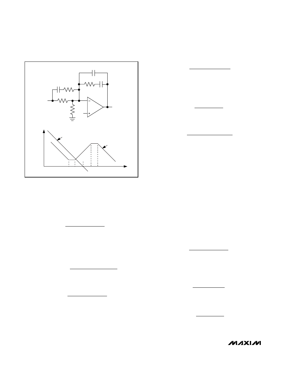
Figure 3. Error Amplifier Compensation Circuit (Closed-Loop
and Error-Amplifier Gain Plot) for Ceramic Capacitors