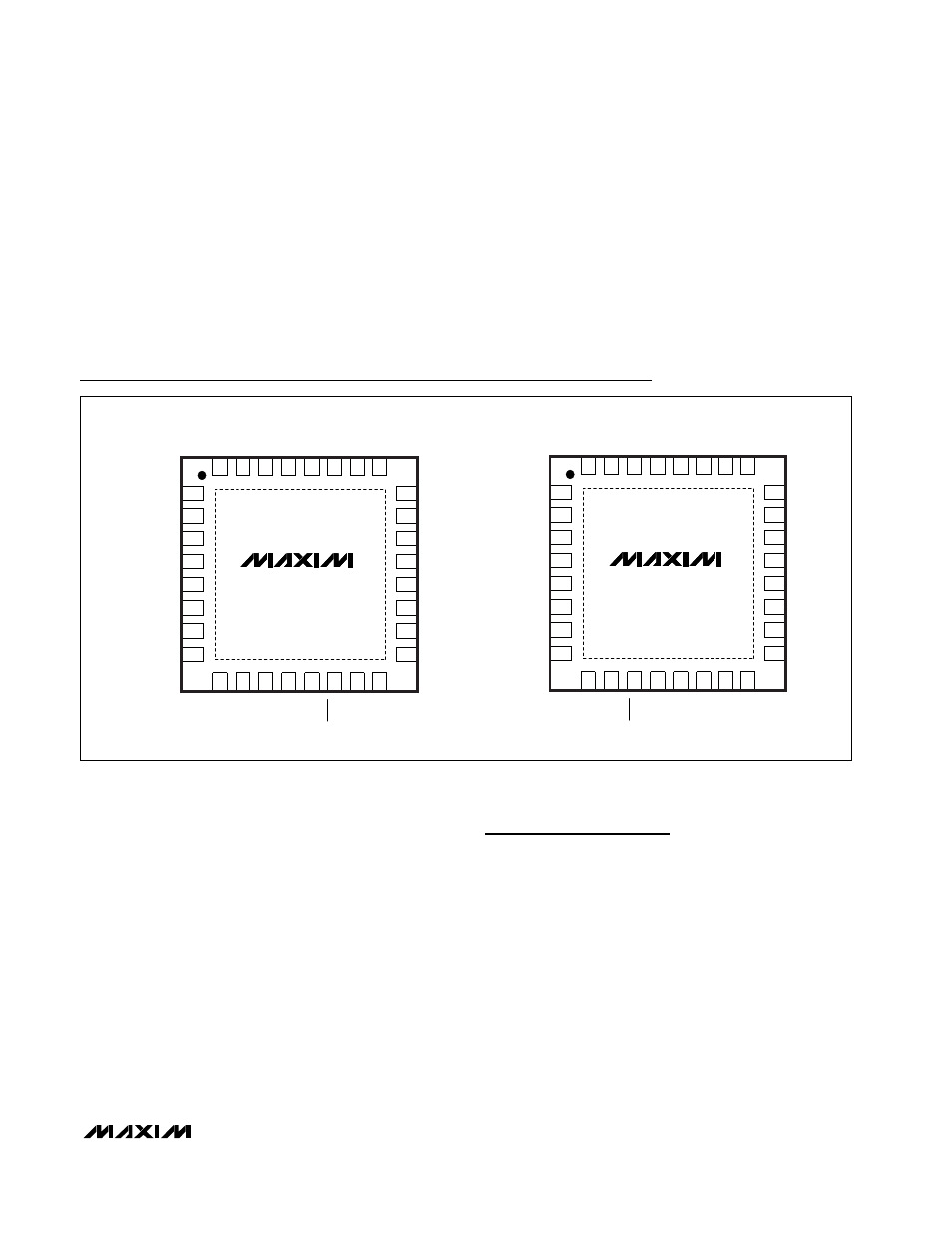
Pin configurations chip information – Rainbow Electronics MAX9704 User Manual
Page 11

Supply Bypassing/Layout
Proper power-supply bypassing ensures low distortion
operation. For optimum performance, bypass V
DD
to
PGND with a 0.1µF capacitor as close to each V
DD
pin
as possible. A low-impedance, high-current power-sup-
ply connection to V
DD
is assumed. Additional bulk
capacitance should be added as required depending on
the application and power-supply characteristics. AGND
and PGND should be star connected to system ground.
Refer to the MAX9704 Evaluation Kit for layout guidance.
MAX9703/MAX9704
15W, Filterless, Spread-Spectrum
Mono/Stereo Class D Amplifiers
______________________________________________________________________________________
11
32
31
30
29
28
27
26
N.C.
N.C.
OUT+
OUT+
OUT-
OUT-
N.C.
25
N.C.
9
10
11
12
13
14
15
REG
AGND
IN-
IN+
SS
G1
16
G2
17
18
19
20
21
22
23
N.C.
FS1
FS2
N.C.
V
DD
V
DD
PGND
8
7
6
5
4
3
2
N.C.
CHOLD
C1P
C1N
V
DD
V
DD
PGND
MAX9703
1
PGND
24
PGND
TOP VIEW
TQFN (5mm x 5mm)
SHDN
32
31
30
29
28
27
26
OUTL+
OUTL+
OUTL-
OUTL-
OUTR+
OUTR+
OUTR-
25
OUTR-
9
10
11
12
13
14
15
INL-
INL+
SS
AGND
INR-
REG
16
INR+
17
18
19
20
21
22
23
G1
G2
FS1
FS2
V
DD
V
DD
PGND
8
7
6
5
4
3
2
N.C.
CHOLD
C1P
C1N
V
DD
V
DD
PGND
MAX9704
1
PGND
24
PGND
TQFN (7mm x 7mm)
SHDN
Pin Configurations
Chip Information
MAX9703 TRANSISTOR COUNT: 3093
MAX9704 TRANSISTOR COUNT: 4630
PROCESS: BiCMOS
