C-interface, digital potentiometers – Rainbow Electronics MAX5419 User Manual
Page 9
MAX5417/MAX5418/MAX5419
256-Tap, Nonvolatile, I
2
C-Interface,
Digital Potentiometers
_______________________________________________________________________________________
9
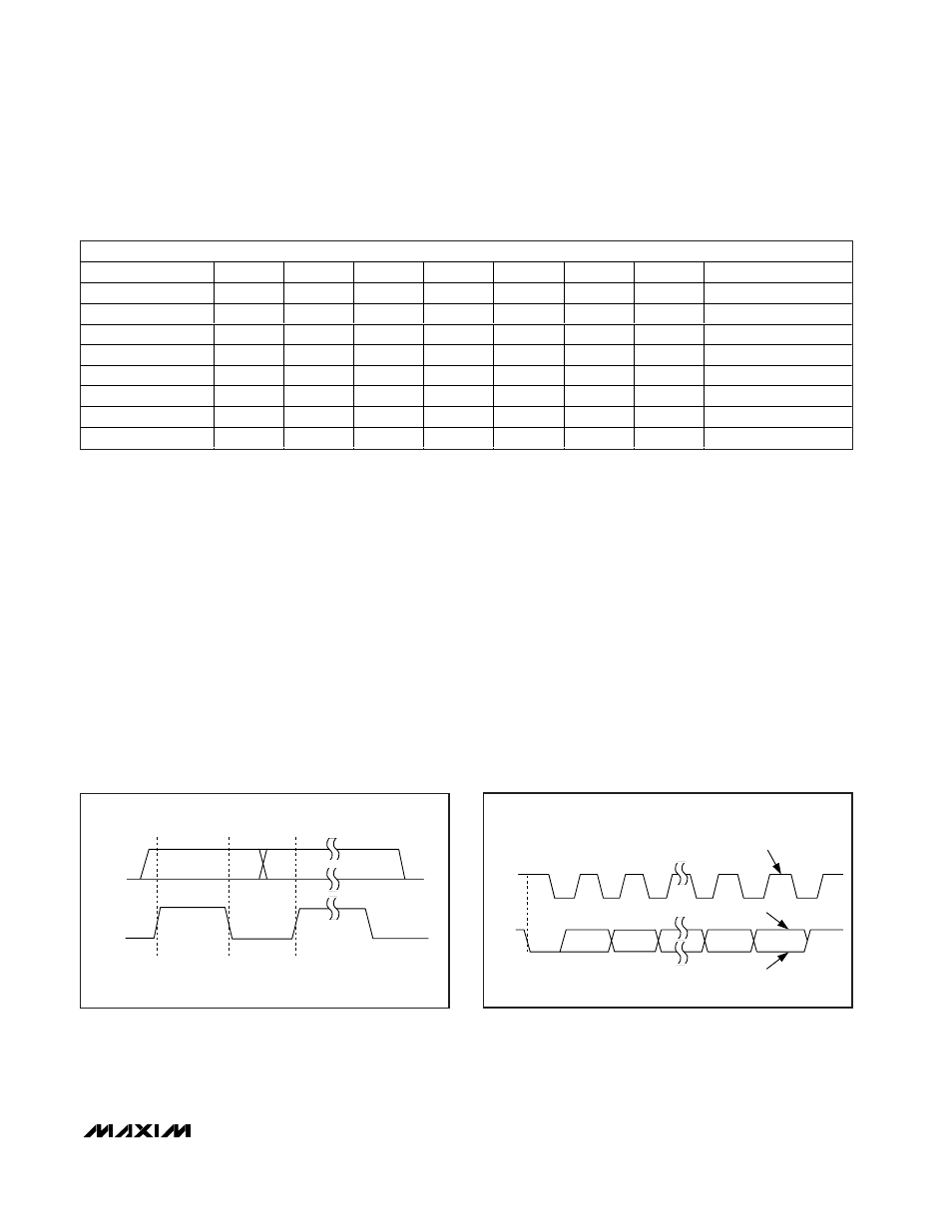
Acknowledge
The acknowledge bit is a clocked 9th bit that the recipient
uses to handshake receipt of each byte of data (Figure
6). Thus, each byte transferred effectively requires 9 bits.
The master generates the 9th clock pulse, and the recipi-
ent pulls down SDA during the acknowledge clock pulse,
so the SDA line is stable low during the high period of the
clock pulse. When the master transmits to the
MAX5417/MAX5418/MAX5419, the devices generate the
acknowledge bit because the MAX5417/MAX5418/
MAX5419 are the recipients.
Slave Address
The MAX5417/MAX5418/MAX5419 have a 7-bit-long
slave address (Figure 4). The 8th bit following the 7-bit
slave address is the NOP/
W bit. Set the NOP/W bit low for
a write command and high for a no-operation command.
The MAX5417/MAX5418/MAX5419 are available in one
of four possible slave addresses (Table 1). The first 4
bits (MSBs) of the MAX5417/MAX5418/MAX5419 slave
addresses are always 0101. The next 2 bits are factory
programmed (see Table 1). Connect the A0 input to
either GND or V
DD
to toggle between two unique
device addresses for a part. Each device must have a
unique address to share the bus. Therefore, a maxi-
mum of eight MAX5417/MAX5418/MAX5419 devices
can share the same bus.
Table 1. MAX5417/MAX5418/MAX5419 Address Codes
ADDRESS BYTE
PART SUFFIX
A6
A5
A4
A3
A2
A1
A0
NOP/W
L
0
1
0
1
0
0
0
NOP/W
L
0
1
0
1
0
0
1
NOP/W
M
0
1
0
1
0
1
0
NOP/W
M
0
1
0
1
0
1
1
NOP/W
N
0
1
0
1
1
0
0
NOP/W
N
0
1
0
1
1
0
1
NOP/W
P
0
1
0
1
1
1
0
NOP/W
P
0
1
0
1
1
1
1
NOP/W
SDA
DATA STABLE,
DATA VALID
CHANGE OF
DATA ALLOWED
SCL
Figure 5. Bit Transfer
1
SCL
START
CONDITION
SDA
2
8
9
CLOCK PULSE FOR
ACKNOWLEDGMENT
ACKNOWLEDGE
NOT ACKNOWLEDGE
Figure 6. Acknowledge