C-interface, digital potentiometers – Rainbow Electronics MAX5419 User Manual
Page 10
MAX5417/MAX5418/MAX5419
256-Tap, Nonvolatile, I
2
C-Interface,
Digital Potentiometers
10
______________________________________________________________________________________
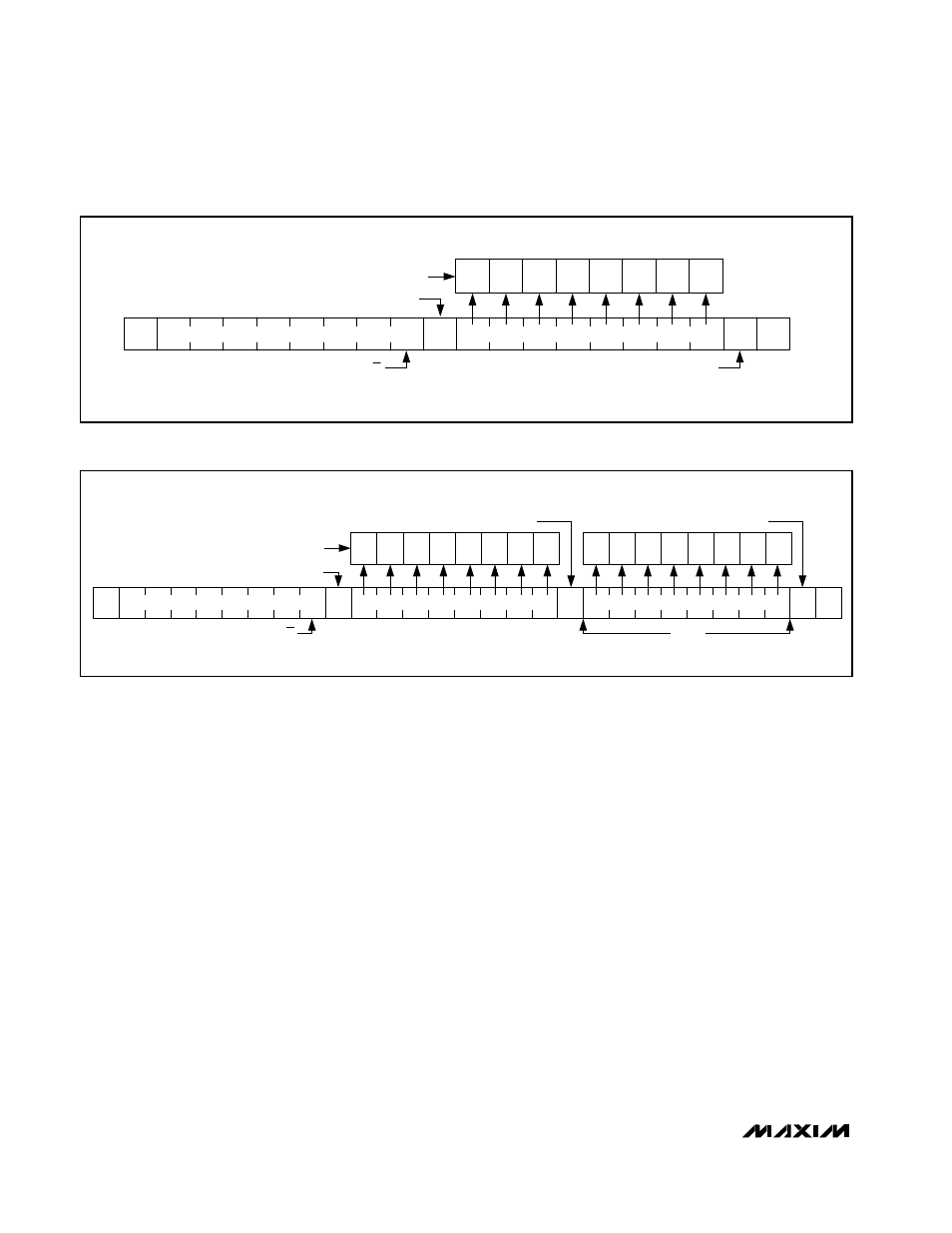
Message Format for Writing
A write to the MAX5417/MAX5418/MAX5419 consists of
the transmission of the device’s slave address with the
8th bit set to zero, followed by at least 1 byte of infor-
mation. The 1st byte of information is the command
byte. The bytes received after the command byte are
the data bytes. The 1st data byte goes into the internal
register of the MAX5417/MAX5418/MAX5419 as select-
ed by the command byte (Figure 8).
Command Byte
Use the command byte to select the source and desti-
nation of the wiper data (nonvolatile or volatile memory
registers) and swap data between nonvolatile and
volatile memory registers (see Table 2).
Command Descriptions
VREG: The data byte writes to the volatile memory reg-
ister and the wiper position updates with the data in the
volatile memory register.
NVREG: The data byte writes to the nonvolatile memory
register. The wiper position is unchanged.
NVxREG: Data transfers from the nonvolatile memory
register to the volatile memory register (wiper position
updates).
VxNVREG: Data transfers from the volatile memory reg-
ister into the nonvolatile memory register.
A
0
SLAVE ADDRESS
CONTROL BYTE
DATA BYTE
ACKNOWLEDGE FROM
MAX5417/MAX5418/MAX5419
NOP/W
1 BYTE
ACKNOWLEDGE FROM
MAX5417/MAX5418/MAX5419
ACKNOWLEDGE FROM
MAX5417/MAX5418/MAX5419
D15
D14 D13 D12 D11 D10
D9
D8
D1
D0
D3
D2
D5
D4
D7
D6
HOW CONTROL BYTE AND DATA BYTE MAP INTO
MAX5417/MAX5418/MAX5419 REGISTERS
S
A
A
P
S
A
0
SLAVE ADDRESS
CONTROL BYTE
ACKNOWLEDGE FROM
MAX5417/MAX5418/MAX5419
NOP/W
ACKNOWLEDGE FROM
MAX5417/MAX5418/MAX5419
D15
D14
D13
D12
D11
D10
D9
D8
CONTROL BYTE IS STORED ON RECEIPT OF STOP CONDITION
A
P
Figure 7. Command Byte Received
Figure 8. Command and Single Data Byte Received