C-interface, digital potentiometers, Pin description, Detailed description – Rainbow Electronics MAX5419 User Manual
Page 7
MAX5417/MAX5418/MAX5419
256-Tap, Nonvolatile, I
2
C-Interface,
Digital Potentiometers
_______________________________________________________________________________________
7
Pin Description
PIN
NAME
FUNCTION
1
V
DD
Power-Supply Input. 2.7V to 5.25V voltage range. Bypass with a 0.1µF capacitor from V
DD
to GND.
2
SCL
I
2
C-Interface Clock Input
3
SDA
I
2
C-Interface Data Input
4
A0
Address Input. Sets the A0 bit in the device ID address.
5
GND
Ground
6
L
Low Terminal
7
W
Wiper Terminal
8
H
High Terminal
—
EP
Exposed Pad
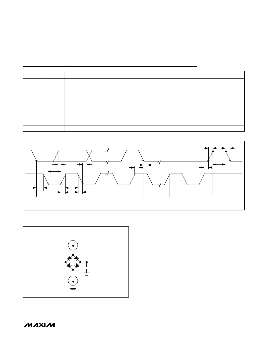
t
HD-STA
t
SU-DAT
t
HIGH
t
R
t
F
t
HD-DAT
t
HD-STA
S
Sr
A
t
SU-STA
t
LOW
t
BUF
t
SU-STO
P
S
t
R
t
F
SCL
SDA
PARAMETERS ARE MEASURED FROM 30% TO 70%.
Detailed Description
The MAX5417/MAX5418/MAX5419 contain a resistor
array with 255 resistive elements. The MAX5417 has a
total end-to-end resistance of 50k
Ω, the MAX5418 has
an end-to-end resistance of 100k
Ω, and the MAX5419
has an end-to-end resistance of 200k
Ω. The
MAX5417/MAX5418/MAX5419 allow access to the high,
low, and wiper terminals for a standard voltage-divider
configuration. H, L, and W can be connected in any
desired configuration as long as their voltages fall
between GND and V
DD
.
A simple 2-wire I
2
C-compatible serial interface moves
the wiper among the 256 tap points. A nonvolatile
memory stores and recalls the stored wiper position in
the nonvolatile memory upon power-up. The nonvolatile
memory is guaranteed for 200,000 wiper store cycles
and 50 years for wiper data retention.
Figure 1. I
2
C Serial-Interface Timing Diagram
V
DD
I
OL
= 3mA
I
OH
= 0mA
V
OUT
400pF
SDA
Figure 2. Load Circuit