C-interface, digital potentiometers, Timing characteristics (continued) – Rainbow Electronics MAX5419 User Manual
Page 4
MAX5417/MAX5418/MAX5419
256-Tap, Nonvolatile, I
2
C-Interface,
Digital Potentiometers
4
_______________________________________________________________________________________
Note 1:
The DNL and INL are measured with the potentiometer configured as a voltage-divider with H = V
DD
and L = GND. The
wiper terminal is unloaded and measured with a high-input-impedance voltmeter.
Note 2:
The DNL and INL are measured with the potentiometer configured as a variable resistor. H is unconnected and L = GND.
For the 5V condition, the wiper terminal is driven with a source current of 80µA for the 50k
Ω configuration, 40µA for the
100k
Ω configuration, and 20µA for the 200kΩ configuration. For the 3V condition the wiper terminal is driven with a source
current of 40µA for the 50k
Ω configuration, 20µA for the 100kΩ configuration, and 10µA for the 200kΩ configuration.
Note 3:
The wiper resistance is measured using the source currents given in Note 2.
Note 4:
The device draws current in excess of the specified supply current when this input is driven with a voltage greater than 0.7
x V
DD
. This is due to the complementary metal-oxide semiconductor (CMOS) shunt current (P- and N-channel output
devices on simultaneously).
Note 5:
Wiper at midscale with a 10pF load. Potentiometer set to midscale, L = GND, an AC source is applied to H, and the output
is measured as 3dB lower than the DC W/H value in dB.
Note 6:
The programming current operates only during power-up and NV writes.
Note 7:
SCL clock period includes rise and fall times t
R
and t
F
. All digital input signals are specified with t
R
= t
F
= 2ns and timed
from a voltage level of (V
IL
+ V
IH
) / 2.
Note 8:
Wiper settling time is the worst-case 0% to 50% rise time measured between consecutive wiper positions. H = V
DD
,
L = GND, and the wiper terminal is unloaded and measured with a 10pF oscilloscope probe (see the Typical Operating
Characteristics for the tap-to-tap switching transient).
Note 9:
An appropriate bus pullup resistance must be selected depending on board capacitance. Refer to the document linked to
this web address: www.semiconductors.philips.com/acrobat/literature/9398/39340011.pdf
Note 10: The idle time begins from the initiation of the stop pulse.
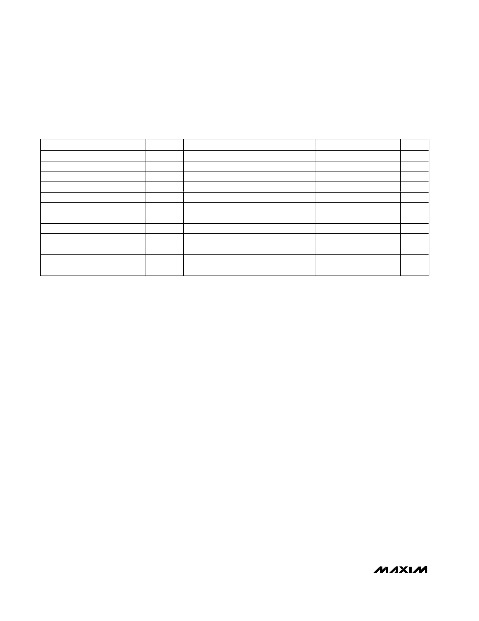
PARAMETER
SYMBOL
CONDITIONS
MIN
TYP
MAX
UNITS
Data Setup Time
t
SU-DAT
100
ns
Data Hold Time
t
HD-DAT
0
0.9
µs
SDA, SCL Rise Time
t
R
300
ns
SDA, SCL Fall Time
t
F
300
ns
Setup Time for STOP Condition
t
SU-STO
0.6
µs
Bus Free Time Between STOP
and START Condition
t
BUF
Minimum power-up rate = 0.2V/ms
1.3
µs
Pulse Width of Spike Suppressed
t
SP
50
ns
Maximum Capacitive Load for
Each Bus Line
C
B
(Note 9)
400
pF
Nonvolatile Store Time
Idle time required after a nonvolatile
memory write (Note 10)
30
ms
TIMING CHARACTERISTICS (continued)
(V
DD
= +2.7V to +5.25V, H = V
DD
, L = GND, T
A
= -40°C to +85°C, unless otherwise noted. Typical values are at V
DD
= +5V, T
A
=
+25°C. See Figures 1 and 2.) (Note 7)