Digital timing characteristics – Rainbow Electronics ADC12041 User Manual
Page 6
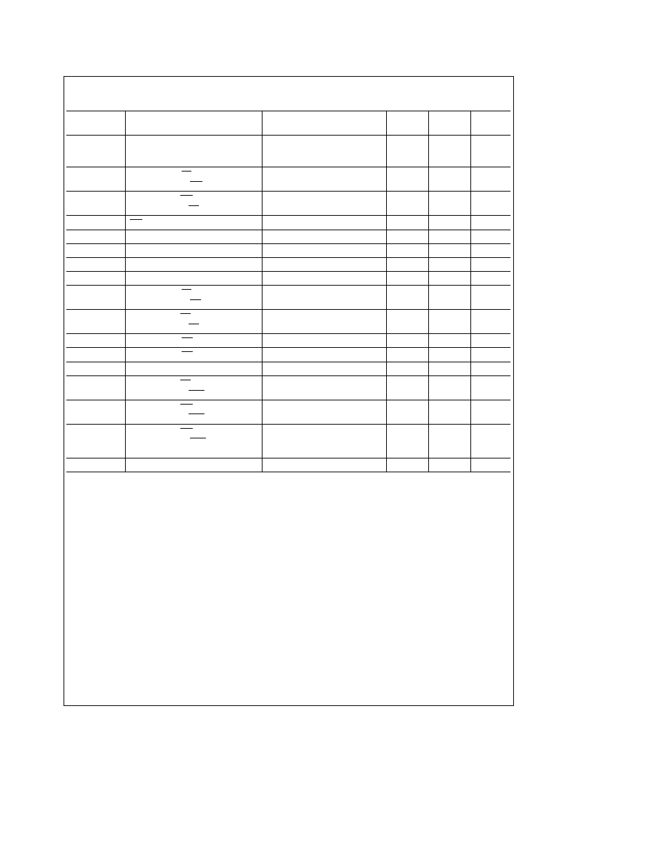
Digital Timing Characteristics
The following specifications apply to the ADC12041 13-bit data bus width
V
A
a
e
V
D
a
e
5V f
CLK
e
12 MHz t
f
e
3 ns and C
L
e
50 pF on data I O lines
Symbol
Parameter
Conditions
Typical
Limits
Unit
(Figure 7)
(Note 10)
(Note 11)
(Limit)
t
TPR
Throughput Rate
Sync-Out Mode (SYNC Bit e ‘‘0’’)
222
kHz
9 Clock Cycles of Acquisition
Time
t
CSWR
Falling Edge of CS
0
ns
to Falling Edge of WR
t
WRCS
Active Edge of WR
0
ns
to Rising Edge of CS
t
WR
WR Pulse Width
20
30
ns (min)
t
WRSETFalling
Write Setup Time
WMODE e ‘‘1’’
20
ns (min)
t
WRHOLDFalling
Write Hold Time
WMODE e ‘‘1’’
5
ns (min)
t
WRSETRising
Write Setup Time
WMODE e ‘‘0’’
20
ns (min)
t
WRHOLDRising
Write Hold Time
WMODE e ‘‘0’’
5
ns (min)
t
CSRD
Falling Edge of CS
0
ns
to Falling Edge of RD
t
RDCS
Rising Edge of RD
0
ns
to Rising Edge of CS
t
RDDATA
Falling Edge of RD to Valid Data
8-Bit Mode (BW Bit e ‘‘0’’)
40
58
ns (max)
t
RDDATA
Falling Edge of RD to Valid Data
13-Bit Mode (BW Bit e ‘‘1’’)
26
44
ns (max)
t
RDHOLD
Read Hold Time
23
32
ns (max)
t
RDRDY
Rising Edge of RD
24
38
ns (max)
to Rising Edge of RDY
t
WRRDY
Active Edge of WR
WMODE e ‘‘1’’
37
60
ns (max)
to Rising Edge of RDY
t
STDRDY
Active Edge of WR
WMODE e ‘‘0’’ Writing the
1 4
2 5
ms (max)
to Falling Edge of RDY
RESET Command into the
Configuration Register
t
SYNC
Minimum SYNC Pulse Width
5
10
ns (min)
Notes on Specifications
Note 1
Absolute Maximum Ratings indicate limits beyond which damage to the device may occur Operating Ratings indicate conditions for which the device is
functional but do not guarantee specific performance limits For guaranteed specifications and test conditions see the Electrical Characteristics The guaranteed
specifications apply only for the test conditions listed Some performance characteristics may degrade when the device is not operated under the listed test
conditions
Note 2
All voltages are measured with respect to GND unless otherwise specified
Note 3
When the input voltage (V
IN
) at any pin exceeds the power supply rails (V
IN
k
GND or V
IN
l
(V
A
a
or V
D
a
)) the current at that pin should be limited to 30
mA The 120 mA maximum package input current limits the number of pins that can safely exceed the power supplies with an input current of 30 mA to four
Note 4
The maximum power dissipation must he derated at elevated temperatures and is dictated by T
Jmax
(maximum junction temperature) i
JA
(package
junction to ambient thermal resistance) and T
A
(ambient temperature) The maximum allowable power dissipation at any temperature is P
Dmax
e
(T
Jmax
b
T
A
)
i
JA
or the number given in the Absolute Maximum Ratings whichever is lower For this device T
Jmax
e
150 C and the typical thermal resistance (i
JA
) of the
ADC12041 in the V package when board mounted is 55 C W and in the SSOP package when board mounted is 130 C W
Note 5
Human body model 100 pF discharged through 1 5 Xk resistor
6