Power supply characteristics, Analog input characteristics, Reference inputs – Rainbow Electronics ADC12041 User Manual
Page 4
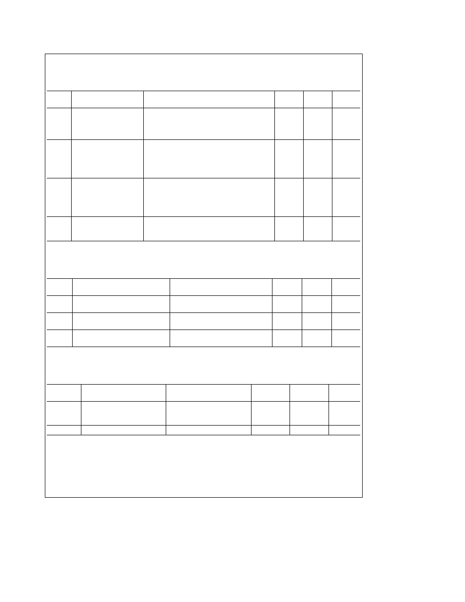
Power Supply Characteristics
The following specifications apply to the ADC12041 for V
A
a
e
V
D
a
e
5V
V
REF
a
e
4 096V V
REF
b
e
0 0V 12-bit a sign conversion mode f
CLK
e
12 0 MHz R
S
e
25X source impedance for V
REF
a
and V
REF
b
1X fully differential input with fixed 2 048V common-mode voltage and minimum acquisition time unless otherwise
specified Boldface limits apply for T
A
e
T
J
e
T
MIN
to T
MAX
all other limits T
A
e
T
J
e
25 C
Symbol
Parameter
Conditions
Typical
Limits
Unit
(Note 10)
(Note 11)
(Limit)
PSS
Power Supply Sensitivity
V
D
a
e
V
A
a
e
5 0V
g
10%
Zero Error
V
REF
a
e
4 096V
g
0 1
LSB
Full-Scale Error
V
REF
b
e
0V
g
0 5
LSB
Linearity Error
g
0 1
LSB
I
D
a
V
D
a
Digital Supply Current
Start Command (Performing a conversion) with SYNC
configured as an input and driven with a 214 kHz
signal Bus width set to 13
f
CLK
e
12 0 MHz Reset Mode
850
m
A
f
CLK
e
12 0 MHz Conversion
2 45
2 6
mA (max)
I
A
a
V
A
a
Analog Supply Current
Start Command (Performing a conversion) with SYNC
configured as an input and driven with a 214 kHz
signal Bus width set to 13
f
CLK
e
12 0 MHz Reset Mode
2 3
mA
f
CLK
e
12 0 MHz Conversion
2 3
4 0
mA (max)
I
ST
Standby Supply Current
Standby Mode
(I
D
a
a
I
A
a
)
f
CLK
e
Stopped
5
15
m
A (max)
f
CLK
e
12 0 MHz
100
120
m
A (max)
Analog Input Characteristics
The following specifications apply to the ADC12041 for V
A
a
e
V
D
a
e
5V
V
REF
a
e
4 096V V
REF
b
e
0 0V 12-Bit a sign conversion mode f
CLK
e
12 0 MHz R
S
e
25X source impedance for
V
REF
a
and V
REF
a
s
1X fully differential input with fixed 2 048V common-mode voltage and minimum acquisition time unless
otherwise specified Boldface limits apply for T
A
e
T
J
e
T
MIN
to T
MAX
all other limits T
A
e
T
J
e
25 C
Symbol
Parameter
Conditions
Typical
Limits
Unit
(Note 10)
(Note 11)
(Limit)
I
IN
V
IN
a
and V
IN
b
Input Leakage Current
V
IN
a
e
5V
0 05
2 0
m
A (max)
V
IN
b
e
0V
b
0 05
R
ON
ADC Input On Resistance
V
IN
e
2 5V
1000
X
Refer to section titled INPUT CURRENT
CV
IN
ADC Input Capacitance
10
pF
Reference Inputs
The following specifications apply to the ADC12041 for V
A
a
e
V
D
a
e
5V V
REF
a
e
4 096V
V
REF
b
e
0 0V 12-bit a sign conversion mode f
CLK
e
12 0 MHz R
S
e
25X source impedance for V
REF
a
and V
REF
b
s
1X fully differential input with fixed 2 048V common-mode voltage and minimum acquisition time unless otherwise specified
Boldface limits apply for T
A
e
T
J
e
T
MIN
to T
MAX
all other limits T
A
e
T
J
e
25 C
Symbol
Parameter
Conditions
Typical
Limits
Unit
(Note 10)
(Note 11)
(Limit)
I
REF
Reference Input Current
V
REF
a
4 096V V
REF
b
e
0V
Analog Input Signal 1 kHz
145
m
A
(Note 20)
80 kHz
136
m
A
C
REF
Reference Input Capacitance
85
pF
4