Pin descriptions and equivalent circuits – Rainbow Electronics ADC14061 User Manual
Page 3

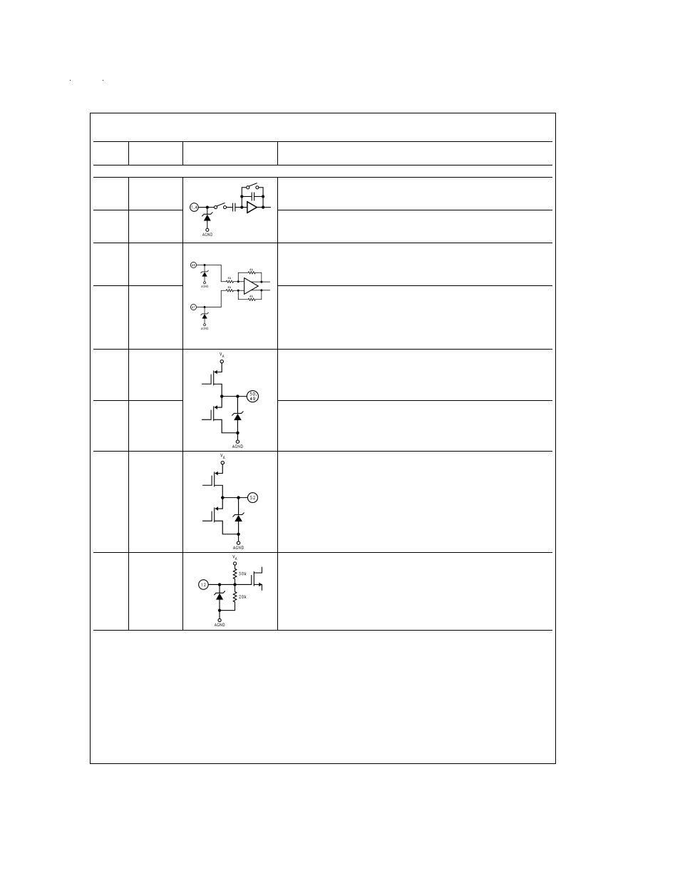
Pin Descriptions and Equivalent Circuits
Pin
No.
Symbol
Equivalent Circuit
Description
Analog I/O
1
V
IN
+
Non-Inverting analog signal Input. With a 2.0V reference voltage and a
2.0V common mode voltage, V
CM
, the input signal voltage range is from
1.0 volt to 3.0 Volts.
4
V
IN
−
Inverting analog signal Input. With a 2.0V reference voltage and a 2.0V
common mode voltage, V
CM
, the input signal voltage range is from 1.0 Volt
to 3.0 Volts. The input signal should be balanced for best performance.
48
V
REF
+
IN
Positive reference input. This pin should be bypassed to AGND with a 0.1
µF monolithic capacitor. V
REF
+ minus V
REF− IN
should be a minimum of
1.8V and a maximum of 2.2V. The full-scale input voltage is equal to
V
REF
+
IN
minus V
REF
−
IN
.
47
V
REF
−
IN
Negative reference input. In most applications this pin should be connected
to AGND and the full reference voltage applied to V
REF
+
IN
. If the
application requires that V
REF
−
IN
be offset from AGND, this pin should be
bypassed to AGND with a 0.1 µF monolithic capacitor. V
REF
+
IN
minus
V
REF− IN
should be a minimum of 1.8V and a maximum of 2.2V. The
full-scale input voltage is equal to V
REF
+
IN
minus V
REF
−
IN
.
50
V
REF
+
OUT
Output of the high impedance positive reference buffer. With a 2.0V
reference input, and with a V
CM
of 2.0V, this pin will have a 3.0V output
voltage. This pin should be bypassed to AGND with a 0.1 µF monolithic
capacitor in parallel with a 10 µF capacitor.
49
REF
−
OUT
The output of the negative reference buffer. With a 2.0V reference and a
V
CM
of 2.0V, this pin will have a 1.0V output voltage. This pin should be
bypassed to AGND with a 0.1 µF monolithic capacitor in parallel with a 10
µF capacitor.
52
V
REF (MID)
Output of the reference mid-point, nominally equal to 0.4 V
A
(2.0V). This
pin should be bypassed to AGND with a 0.1 µF monolithic capacitor. This
voltage is derived from V
CM
.
51
V
CM
Input to the common mode buffer, nominally equal to 40% of the supply
voltage (2.0V). This pin should be bypassed to AGND with a 0.1 µF
monolithic capacitor. Best performance is obtained if this pin is driven with
a low impedance source of 2.0V.
www.national.com
3
