Applications information – Rainbow Electronics ADC14061 User Manual
Page 15

Applications Information
(Continued)
To avoid signal clipping and distortion, V
REF
+
OUT
should not
exceed 3.3V, V
REF
−
OUT
should not be below 750 mV and
V
CM
should be held in the range of 1.8V to 2.2V.
3.2 The /EOC output goes low to indicate the presence of
valid data at the output data lines. Valid data is present the
entire time that this signal is low except during reset. Corrupt
or irrelevant data may appear at the data outputs when the
RESET pin or the CAL pin is high.
3.3 The Data Outputs are TTL/CMOS compatible. The out-
put data format is two’s complement. Valid data is present at
these outputs while the EOC pin is low. While the t
EOCL
time
and the t
DATA_VALID
time provide information about output
timing, a simple way to capture a valid output is to latch the
data on the rising edge of the CLOCK (pin 10).
Also helpful in minimizing noise due to output switching is to
minimize the load currents at the digital outputs. This can be
done by connecting buffers between the ADC outputs and
any other circuitry. Only one input should be connected to
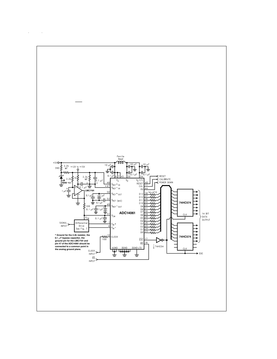
each output pin. Additionally, inserting series resistors of 47
or 56 Ohms at the digital outputs, close to the ADC pins, will
isolate the outputs from other circuitry and limit output cur-
rents. (See
Figure 6
).
4.0 POWER SUPPLY CONSIDERATIONS
Each power supply pin should be bypassed with a parallel
combination of a 10 µF capacitor and a 0.1 µF ceramic chip
capacitor. The chip capacitors should be within
1
⁄
2
centimeter
of the power pins. Leadless chip capacitors are preferred be-
cause they provide low lead inductance.
While a single 5V source is used for the analog and digital
supplies of the ADC14061, these supply pins should be well
isolated from each other to prevent any digital noise from be-
ing coupled to the analog power pins. Supply isolation with
ferrite beads is shown in
Figure 6
and
Figure 8
.
As is the case with all high-speed converters, the ADC14061
is sensitive to power supply noise. Accordingly, the noise on
the analog supply pin should be kept below 100 mV
P-P
.
No pin should ever have a voltage on it that is in excess of
the supply voltages, not even at power up.
The V
D
I/O provides power for the output drivers and may be
operated from a supply in the range of 3.0V to the V
D
supply
(nominal 5V). This can simplify interfacing to 3.0 Volt devices
and systems. Powering V
D
I/O from 3 Volts will also reduce
power consumption and noise generation due to output
switching. DO NOT operate the V
D
I/O at a voltage higher
than V
D
or V
A
.
DS100103-19
FIGURE 6. Simple application circuit with single-ended to differential buffer.
www.national.com
15
