Driving capacitive loads, Power-supply bypassing and layout – Rainbow Electronics MAX4244 User Manual
Page 13

value, based on driving the output voltage to within
50mV, 100mV, and 200mV of either power-supply rail.
For example, a MAX4241 running from a single +1.8V
supply, operating at T
A
= +25°C, can source 240µA to
within 100mV of V
CC
and is capable of driving a 7k
Ω
load resistor to V
EE
:
The same application can drive a 3.3k
Ω
load resistor
when terminated in V
CC
/ 2 (+0.9V in this case).
Driving Capacitive Loads
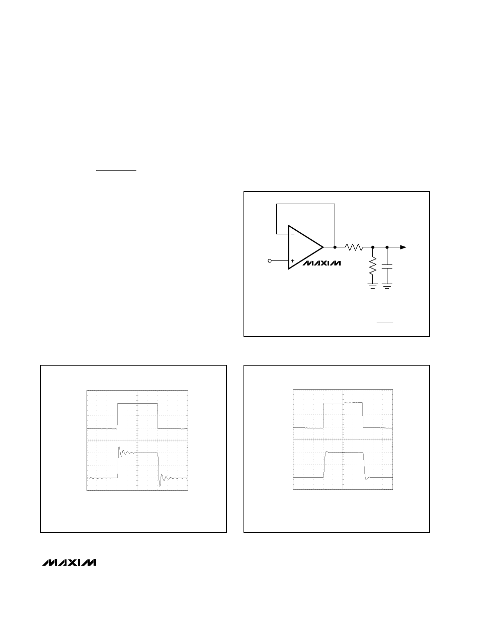
The MAX4240–MAX4244 are unity-gain stable for loads
up to 200pF (see Load Resistor vs. Capacitive Load
graph in
Typical Operating Characteristics
). Applica-
tions that require greater capacitive drive capability
should use an isolation resistor between the output and
the capacitive load (Figure 8). Note that this alternative
results in a loss of gain accuracy because R
ISO
forms a
voltage divider with the load resistor.
Power-Supply Bypassing and Layout
The MAX4240–MAX4244 family operates from either a
single +1.8V to +5.5V supply or dual ±0.9V to ±2.75V
supplies. For single-supply operation, bypass the
power supply with a 100nF capacitor to V
EE
(in this
case GND). For dual-supply operation, both the V
CC
and V
EE
supplies should be bypassed to ground with
separate 100nF capacitors.
Good PC board layout techniques optimize perfor-
mance by decreasing the amount of stray capacitance
at the op amp’s inputs and output. To decrease stray
capacitance, minimize trace lengths by placing exter-
nal components as close as possible to the op amp.
Surface-mount components are an excellent choice.
R =
1.8V - 0.1V
240 A
7k to V
L
EE
µ
=
Ω
MAX4240–MAX4244
Single/Dual/Quad, +1.8V/10µA, SOT23,
Beyond-the-Rails Op Amps
______________________________________________________________________________________
13
R
ISO
C
L
R
L
MAX4240
MAX4241
MAX4242
MAX4243
MAX4244
A
V
=
R
L
≈
1
R
L
+ R
ISO
Figure 8a Using a Resistor to Isolate a Capacitive Load from
the Op Amp
50mV/div
IN
OUT
50mV/div
MAX4240-44 fig08b
100
µ
s/div
R
ISO
= NONE, R
L
= 100k
Ω
, C
L
= 700pF
Figure 8b. Pulse Response without Isolating Resistor
50mV/div
IN
OUT
50mV/div
MAX4240-44 fig08c
100
µ
s/div
R
ISO
= 1k
Ω
, R
L
= 100k
Ω
, C
L
= 700pF
Figure 8c. Pulse Response with Isolating Resistor
