Detailed description – Rainbow Electronics MAX4244 User Manual
Page 10
MAX4240–MAX4244
Single/Dual/Quad, +1.8V/10µA, SOT23,
Beyond-the-Rails Op Amps
10
______________________________________________________________________________________
_______________Detailed Description
Beyond-the-Rails Input Stage
The MAX4240–MAX4244 have Beyond-the-Rails™ inputs
and Rail-to-Rail
®
output stages that are specifically
designed for low-voltage, single-supply operation. The
input stage consists of separate NPN and PNP differen-
tial stages, which operate together to provide a com-
mon-mode range extending to 200mV beyond both
supply rails. The crossover region of these two pairs
occurs halfway between V
CC
and V
EE
. The input offset
voltage is typically 200µV. Low operating supply voltage,
low supply current, beyond-the-rails common-mode
input range, and rail-to-rail outputs make this family of
operational amplifiers an excellent choice for precision or
general-purpose, low-voltage battery-powered systems.
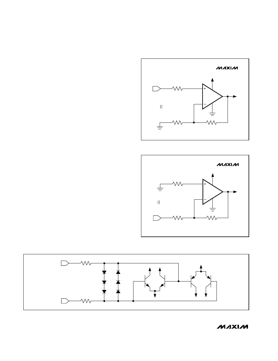
Since the input stage consists of NPN and PNP pairs,
the input bias current changes polarity as the common-
mode voltage passes through the crossover region.
Match the effective impedance seen by each input to
reduce the offset error caused by input bias currents
flowing through external source impedances (Figures
1a and 1b). The combination of high source impedance
plus input capacitance (amplifier input capacitance
plus stray capacitance) creates a parasitic pole that
produces an underdamped signal response. Reducing
input capacitance or placing a small capacitor across
the feedback resistor improves response in this case.
The MAX4240–MAX4244 family’s inputs are protected
from large differential input voltages by internal 2.2k
Ω
series resistors and back-to-back triple-diode stacks
across the inputs (Figure 2). For differential input volt-
ages (much less than 1.8V), input resistance is typically
45M
Ω
. For differential input voltages greater than 1.8V,
input resistance is around 4.4k
Ω
, and the input bias
current can be approximated by the following equation:
I
BIAS
= (V
DIFF
- 1.8V) / 4.4k
Ω
R3
V
IN
R3 = R1 R2
R1
R2
MAX4240
MAX4241
MAX4242
MAX4243
MAX4244
Figure 1a. Minimizing Offset Error Due to Input Bias Current
(Noninverting)
R3
R3 = R1 R2
R1
R2
MAX4240
MAX4241
MAX4242
MAX4243
MAX4244
V
IN
Figure 1b. Minimizing Offset Error Due to Input Bias Current
(Inverting)
2.2k
2.2k
IN-
IN+
Figure 2. Input Protection Circuit