Rainbow Electronics MAX8625A User Manual
Page 9
MAX8625A
High-Efficiency, Seamless Transition,
Step-Up/Down DC-DC Converter
_______________________________________________________________________________________
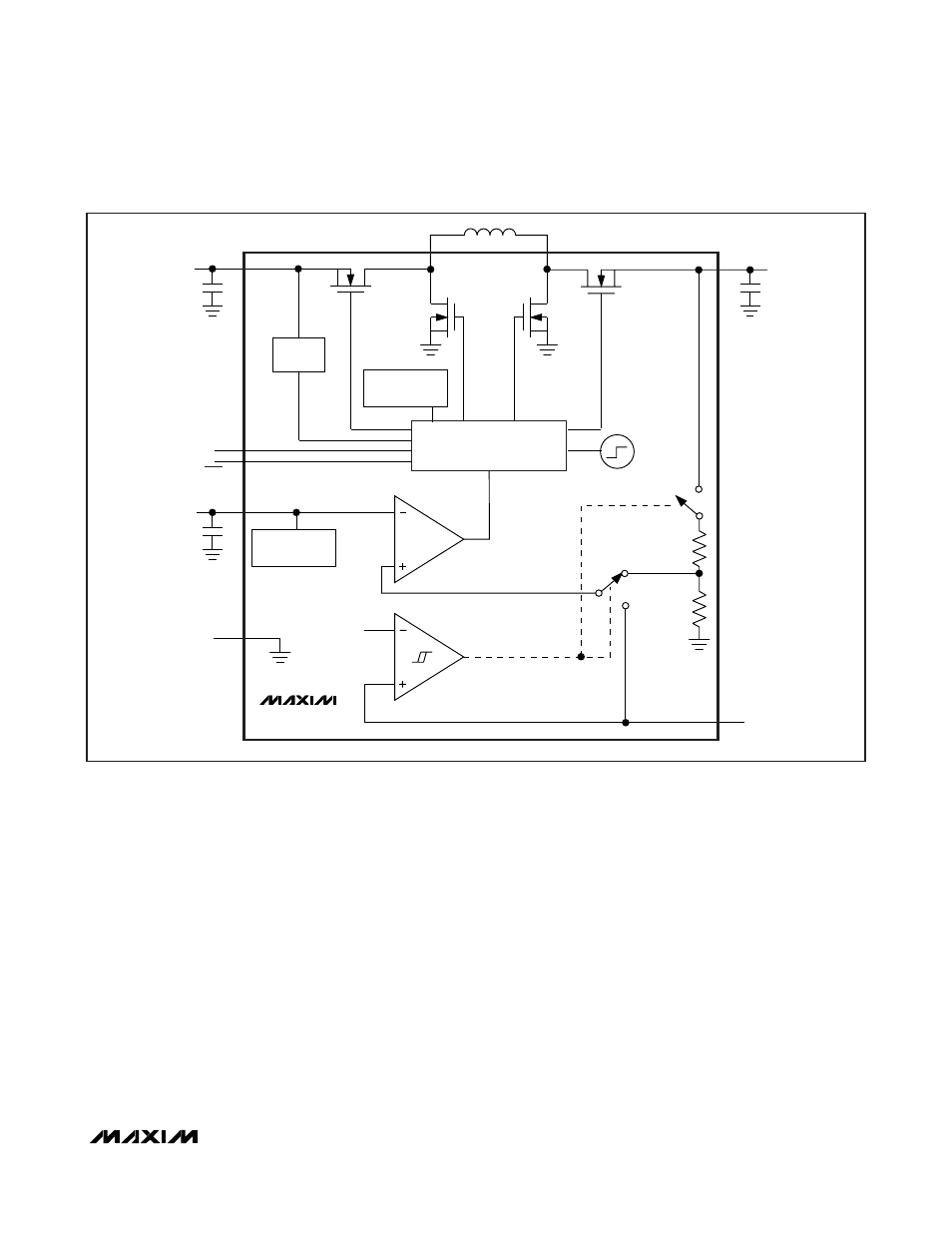
9
times. This reduces the ripple and removes any mode
transitions from boost-only or buck-only to hybrid modes
as seen in competing H-bridge converters.
The time spent in each phase is set by a PWM con-
troller, using timers and/or peak-current regulation on a
cycle-by-cycle basis. The heart of the PWM control
block is a comparator that compares the output volt-
age-error feedback signal and the sum of the current-
sense and slope compensation signals. The current-
mode control logic regulates the inductor current as a
function of the output error voltage signal. The current-
sense signal is monitored across the MOSFETs (P1, N1,
and N2). A fixed time delay of approximately 30ns
occurs between turning the P1 and N2 MOSFETs off,
and turning the N1 and P2 MOSFETs on. This dead
time prevents efficiency loss by preventing “shoot-
through” current.
Step-Down Operation (V
IN
> V
OUT
)
During medium and heavy loads and V
IN
> V
OUT
,
MOSFETs P1 and N2 turn on to begin phase 1 at the
clock edge and ramp up the inductor current. The
duration of phase 1 is set by an internal timer. During
phase 2, N2 turns off, and P2 turns on to further ramp
up inductor current and also transfer charge to the out-
put. This slow charge phase is terminated on a clock
edge and P1 is turned off. The converter now enters the
fast discharge phase (phase 3). In phase 3, N1 turns
on and the inductor current ramps down to the valley
current-regulation point set by the error signal. At the
end of phase 3, both P2 and N1 turn off and another
phase 1 is initiated and the cycle repeats.
With SKIP asserted low, during light loads when induc-
tor current falls to zero in phase 3, the converter switch-
es to phase 4 to reduce power consumption and avoid
Figure 1. Simplified Block Diagram
MAX8625
Gm
FB
UVLO
P1
CURRENT SENSE
REFERENCE
PWM/PFM
CONTROL
P1
P2
N2
OUT
IN
REF
LX1
LX2
N1
ON
SKIP
OSCILLATOR
GND
1.25V
125mV