Rainbow Electronics MAX8625A User Manual
Page 2
MAX8625A
High-Efficiency, Seamless Transition,
Step-Up/Down DC-DC Converter
2
_______________________________________________________________________________________
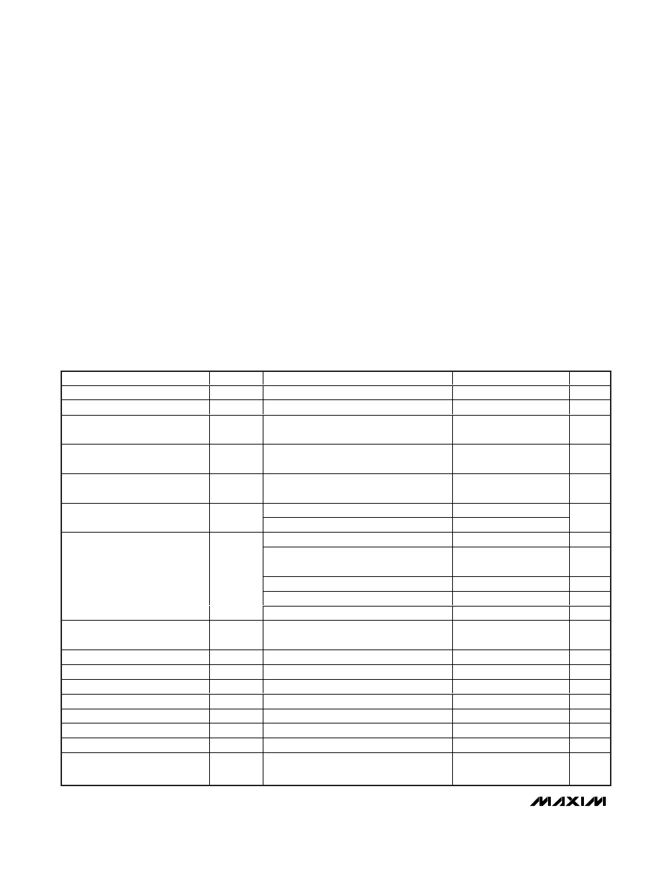
ABSOLUTE MAXIMUM RATINGS
ELECTRICAL CHARACTERISTICS
(V
IN
= 3.6V, ON = SKIP = IN, FB = GND, V
OUT
= 3.3V, LX_ unconnected, C
REF
= C5 = 0.1µF to GND, Figure 4. T
A
= -40°C to +85°C.
Typical values are at T
A
= +25°C, unless otherwise noted.) (Note 2)
Stresses beyond those listed under “Absolute Maximum Ratings” may cause permanent damage to the device. These are stress ratings only, and functional
operation of the device at these or any other conditions beyond those indicated in the operational sections of the specifications is not implied. Exposure to
absolute maximum rating conditions for extended periods may affect device reliability.
IN, OUT, SKIP, ON to GND ......................................-0.3V to +6V
REF, FB, to GND...............................................-0.3V, (IN + 0.3V)
LX2, LX1 (Note 1) .........................................................±1.5A
RMS
Continuous Power Dissipation (T
A
= +70°C)
Single-Layer Board (derate 18.5mW/°C
above T
A
= +70°C) ...................................................1482mW
Operating Temperature Range ...........................-40°C to +85°C
Junction Temperature ......................................................+150°C
Storage Temperature Range .............................-65°C to +150°C
Lead Temperature (soldering, 10s) .................................+300°C
PARAMETER
SYMBOL
CONDITIONS
MIN
TYP
MAX
UNITS
Supply Range
V
IN
2.5
5.5
V
UVLO Threshold
UVLO
V
IN
rising, 60mV hysteresis
2.20
2.49
V
Quiescent Supply Current, FPWM
Mode, Switching
I
IN
No load, V
OUT
= 3.2V
15
22
mA
Quiescent Supply Current, Skip
Mode, Switching
I
IN
SKIP = GND, no load
37
µA
Quiescent Supply Current, No
Switching, Skip Mode
I
IN
SKIP = GND, FB = 1.3V
35
45
µA
ON = GND, T
A
= +25°C
0.1
1
Shutdown Supply Current
I
IN
T
A
= +85°C
0.2
µA
PWM mode, V
IN
= 2.5V to 5.5V
3.30
V
I
OUT
= 0 to 0.5A, V
IN
= 2.5V to 5.5V,
T
A
= -40°C to +85°C (Note 3)
-1
+1
%
SKIP mode, valley regulation value
3.28
V
Average skip voltage
3.285
Output Voltage Accuracy
(Fixed Output)
Load step +0.5A
-3
%
Output Voltage Range
(Adjustable Output)
1.25
4.00
V
Maximum Output Current
V
IN
= 3.6V
0.80
A
Soft-Start
L = 3.3µH; C
OUT
= C3 + C4 = 44µF
250
mA/ms
Load Regulation
I
OUT
= 0 to 500mA
0.1
%/mA
Line Regulation
V
IN
= 2.5V to 5.5V
0.03
%/V
OUT Bias Current
I
OUT
V
OUT
= 3.3V
3
µA
REF Output Voltage
V
REF
V
IN
= 2.5V to 5.5V
1.244
1.25
1.256
V
REF Load Regulation
I
REF
= 10µA
1
mV
FB Feedback Threshold
V
FB
I
OUT
= 0 to full load, PWM mode; V
IN
= 2.5V
to 5.5V
1.244
1.25
1.258
V
Note 1: LX1 and LX2 have internal clamp diodes to IN, PGND and OUT, PGND, respectively. Applications that forward bias these
diodes should take care not to exceed the device's power-dissipation limits.