Detailed description, Pin description – Rainbow Electronics MAX8625A User Manual
Page 8
MAX8625A
High-Efficiency, Seamless Transition,
Step-Up/Down DC-DC Converter
8
_______________________________________________________________________________________
Detailed Description
The MAX8625A step-up/down architecture employs a
true H-bridge topology that combines a boost converter
and a buck converter topology using a single inductor
and output capacitor (Figure 1). The MAX8625A utilizes
a pulse-width modulated (PWM), current-mode control
scheme and operates at a 1MHz fixed frequency to
minimize external component size. A proprietary
H-bridge design eliminates mode changes when transi-
tioning from buck to boost operation. This control
scheme provides very low output ripple using a much
smaller inductor than a conventional H-bridge, while
avoiding glitches that are commonly seen during mode
transitions with competing devices.
The MAX8625A switches at an internally set frequency
of 1MHz, allowing for tiny external components. Internal
compensation further reduces the external component
count in cost- and space-sensitive applications. The
MAX8625A is optimized for use in HDDs, DSCs, and
other devices requiring low-quiescent current for opti-
mal light-load efficiency and maximum battery life.
Control Scheme
The MAX8625A basic noninverting step-up/down con-
verter operates with four internal switches. The control
logic determines which two internal MOSFETs operate
to maintain the regulated output voltage. Unlike a tradi-
tional H-bridge, the MAX8625A utilizes smaller peak-
inductor currents, thus improving efficiency and
lowering input/output ripple.
The MAX8625A uses three operating phases during
each switching cycle. In phase 1 (fast-charge), the
inductor current ramps up with a di/dt of V
IN
/L. In phase
2 (slow charge/discharge), the current either ramps up
or down depending on the difference between the input
voltage and the output voltage (V
IN
- V
OUT
)/L. In phase 3
(discharge), the inductor current discharges at a rate of
V
OUT
/L through MOSFETs P2 and N1 (see Figure 1). An
additional fourth phase (phase 4: hold) is entered when
the inductor current falls to zero during phase 3. This
fourth phase is only used during skip operation.
The state machine (Figure 2) decides which phase to
use and when to switch phases. The converter goes
through the first three phases in the same order at all
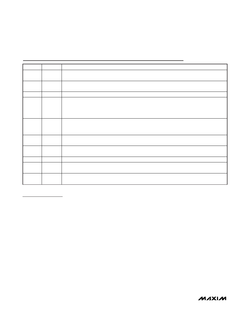
Pin Description
PIN
NAME
FUNCTION
1, 2
LX1
Inductor Connection 1. Connect the inductor between LX1 and LX2. Both LX1 pins must be connected
together externally. LX1 is internally connected to GND during shutdown.
3, 4
LX2
Inductor Connection 2. Connect the inductor between LX1 and LX2. Both LX2 pins must be connected
together externally. LX2 is internally connected to GND during shutdown.
5
ON
Enable Input. Connect ON to the input or drive high to enable the IC. Drive ON low to disable the IC.
6
SKIP
Mode Select Input. Connect SKIP to GND to enable skip mode. This mode provides the best overall
efficiency curve.
Connect SKIP to IN to enable forced-PWM mode. This mode provides the lowest noise, but reduces light-
load efficiency compared to skip mode.
7
FB
Feedback Input. Connect to ground to set the fixed 3.3V output. Connect FB to the center tap of an
external resistor-divider from the output to GND to set the output voltage to a different value. V
FB
regulates
to 1.25V.
8
REF
Reference Output. Bypass REF to GND with a 0.1µF ceramic capacitor. V
REF
is 1.25V and is internally
pulled to GND during shutdown.
9, 10
OUT
Power Output. Bypass OUT to GND with two 22µF ceramic capacitors. Both OUT pins must be connected
together externally.
11, 12
GND
Ground. Connect the exposed pad and GND directly under the IC.
13, 14
IN
Power-Supply Input. Bypass IN to GND with two 22µF ceramic capacitors. Connect IN to a 2.5V to 5.5V
supply. Both IN pins must be connected together externally.
—
EP
Exposed Pad. Connect to GND directly under the IC. Connect to a large ground plane for increased
thermal performance.