Applications information, Selecting the output voltage, Calculating maximum output current – Rainbow Electronics MAX8625A User Manual
Page 12: Capacitor selection, Inductor selection, Pcb layout and routing
MAX8625A
High-Efficiency, Seamless Transition,
Step-Up/Down DC-DC Converter
12
______________________________________________________________________________________
Applications Information
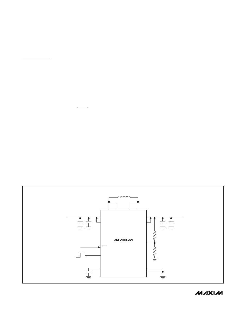
Selecting the Output Voltage
The MAX8625A output is nominally fixed at 3.3V.
Connect FB to GND to select the internally fixed-output
voltage. For an adjustable output voltage, connect FB
to the center tap of an external resistor-divider connect-
ed from the output to GND (R1 and R2 in Figure 3).
Select 100k
Ω for R2 and calculate R1 using the follow-
ing equation:
where V
FB
= 1.25V and V
OUT
is the desired output reg-
ulation voltage. V
OUT
must be between 1.25V and 4V.
Note that the minimum output voltage is limited by the
minimum duty cycle. V
OUT
cannot be below 1.25V.
Calculating Maximum Output Current
The maximum output current provided by the MAX8625A
circuit depends on the inductor value, switching frequen-
cy, efficiency, and input/output voltage.
See the
Typical Operating Characteristics
section for
the Maximum Load Current vs. Input Voltage graph.
Capacitor Selection
The input and output ripple currents are both discontin-
uous in this topology. Therefore, select at least two
22µF ceramic capacitors at the input. Select two 22µF
ceramic output capacitors. For best stability over a
wide temperature range, use X5R or better dielectric.
Inductor Selection
The recommended inductance range for the
MAX8625A is 3.3µH to 4.7µH. Larger values of L give a
smaller ripple, while smaller L values provide a better
transient response. This is because, for boost and step-
up/down topologies, the crossover frequency is
inversely proportional to the value of L for a given load
and input voltage. The MAX8625A is internally compen-
sated, and therefore, the choice of power components
for stable operation is bounded. A 3.3µH inductor with
2A rating is recommended for the 3.3V fixed output with
0.8A load.
PCB Layout and Routing
Good PCB layout is important to achieve optimal per-
formance from the MAX8625A. Poor design can cause
excessive conducted and/or radiated noise.
Conductors carrying discontinuous currents and any
high-current path should be made as short and wide as
possible. Keep the feedback network (R1 and R2) very
close to the IC, preferably within 0.2 inches of the FB
and GND pins. Nodes with high dv/dt (switching
nodes) should be kept as small as possible and routed
away from FB. Connect the input and output capacitors
as close as possible to the IC. Refer to the MAX8625A
evaluation kit for a PCB layout example.
R
k
V
V
OUT
FB
1
100
1
=
×
−
⎛
⎝⎜
⎞
⎠⎟
Ω
Figure 3. Typical Application Circuit (Adjustable Output)
U1
MAX8625A
R2
100k
Ω
R1
140k
Ω
IN
SKIP
IN
OUT
FB
OUT
LX1
LX1
LX2
LX2
1
2
13
14
6
ON
5
REF
8
3
4
L
3.3
μH
C1, C2
22
μF
C5
0.1
μF
9
7
10
C3, C4
22
μF
INPUT
2.7V TO 5.5V
MODE
SELECTION
INPUT
OUTPUT
3V
OFF
ON
GND
GND
11
12