Applications information – Rainbow Electronics MAX5189 User Manual
Page 9
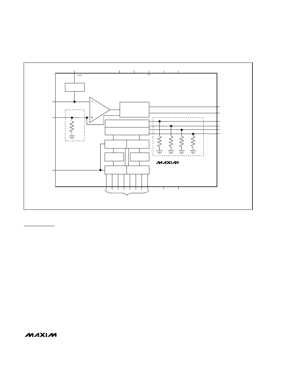
MAX5186/MAX5189
Dual, 8-Bit, 40MHz, Current/Voltage,
Simultaneous-Output DACs
_______________________________________________________________________________________
9
Applications Information
Static and Dynamic
Performance Definitions
Integral Nonlinearity
Integral nonlinearity (INL) (Figure 5a) is the deviation of
the values on an actual transfer function from either a
best-straight-line fit (closest approximation to the actual
transfer curve) or a line drawn between the endpoints
of the transfer function once offset and gain errors have
been nullified. For a DAC, the deviations are measured
every single step.
Differential Nonlinearity
Differential nonlinearity (DNL) (Figure 5b) is the differ-
ence between an actual step height and the ideal value
of 1LSB. A DNL error specification of less than 1LSB
guarantees no missing codes and a monotonic transfer
function.
Offset Error
Offset error (Figure 5c) is the difference between the
ideal and the actual offset point. For a DAC, the offset
point is the step value when the digital input is zero.
This error affects all codes by the same amount and
can usually be compensated by trimming.
Gain Error
Gain error (Figure 5d) is the difference between the
ideal and the actual full-scale output voltage on the
transfer curve after nullifying the offset error. This error
alters the slope of the transfer function and corre-
sponds to the same percentage error in each step.
Settling Time
Settling time is the amount of time required from the start
of a transition until the DAC output settles its new output
value to within the converter’s specified accuracy.
9.6k*
Ω
REFR
REFO
1.2V REF
REN
CURRENT-
SOURCE ARRAY
DAC1 SWITCHES
DAC2 SWITCHES
400
Ω*
OUT1P
OUT1N
OUT2N
OUT2N
400
Ω*
400
Ω* 400Ω*
MSB
DECODE
CLK
OUTPUT
LATCHES
OUTPUT
LATCHES
INPUT
LATCHES
*INTERNAL 400
Ω AND 9.6kΩ
RESISTORS FOR MAX5189 ONLY.
INPUT
LATCHES
AV
DD
AGND
CS
DACEN
PD
DV
DD
DGND
CREF1
CREF2
MAX5186
MAX5189
MSB
DECODE
D7–D0
Figure 1. Functional Diagram