Rainbow Electronics MAX5189 User Manual
Page 13
MAX5186/MAX5189
Dual, 8-Bit, 40MHz, Current/Voltage,
Simultaneous-Output DACs
______________________________________________________________________________________
13
ence, power-supply, and ground connections, which
may affect dynamic specifications like signal-to-noise
ratio or SFDR. In addition, electromagnetic interference
(EMI) can either couple into or be generated by the
MAX5186/MAX5189. Therefore, grounding and power-
supply decoupling guidelines for high-speed, high-fre-
quency applications should be closely followed.
First, a multilayer printed circuit (PC) board with sepa-
rate ground and power-supply planes is recommend-
ed. High-speed signals should be run on controlled
impedance lines directly above the ground plane.
Since the MAX5186/MAX5189 have separate analog
and digital ground buses (AGND and DGND, respec-
tively), the PC board should also have separate analog
and digital ground sections with only one point con-
necting the two. Digital signals should run above the
digital ground plane, and analog signals should run
above the analog ground plane. Digital signals should
be kept far away from the sensitive analog reference
and clock input.
Both devices have two power-supply inputs: analog
V
DD
(AV
DD
) and digital V
DD
(DV
DD
). Each AV
DD
input
should be decoupled with parallel 10µF and 0.1µF
ceramic-chip capacitors. These capacitors should be
as close to the pin as possible, and their opposite ends
should be as close to the ground plane as possible.
The DV
DD
pins should also have separate 10µF and
0.1µF capacitors adjacent to their respective pins. Try
to minimize analog load capacitance for proper opera-
tion. For best performance, it is recommended to
REN
AGND
DGND
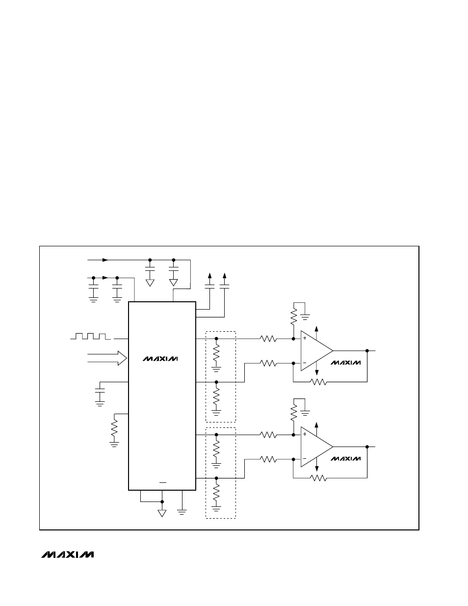
**MAX5186 ONLY
OUT1P
CREF2
CREF1
CLK
OUT1N
OUT2P
OUT2N
0.1
µF
0.1
µF
0.1
µF
DV
DD
AV
DD
AV
DD
AV
DD
R
SET
**
*400
Ω RESISTORS INTERNAL TO MAX5189 ONLY.
MAX5186
MAX5189
10
µF
+3V
+3V
0.1
µF
0.1
µF
REFR
REFO
D0–D7
10
µF
400
Ω
400
Ω
+5V
-5V
402
Ω
402
Ω
402
Ω
402
Ω
*
*
*
OUTPUT 1
MAX4108
400
Ω
*
400
Ω
+5V
-5V
402
Ω
402
Ω
402
Ω
402
Ω
OUTPUT 2
MAX4108
+
+
Figure 6. Differential to Single-Ended Conversion Using a Low-Distortion Amplifier