Rainbow Electronics MAX5189 User Manual
Page 2
MAX5186/MAX5189
Dual, 8-Bit, 40MHz, Current/Voltage,
Simultaneous-Output DACs
2
_______________________________________________________________________________________
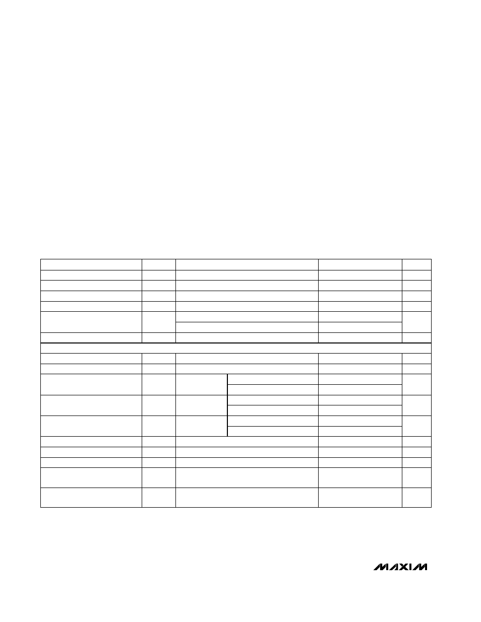
ABSOLUTE MAXIMUM RATINGS
ELECTRICAL CHARACTERISTICS
(AV
DD
= DV
DD
= +3V ±10%, AGND = DGND = 0, f
CLK
= 40MHz, I
FS
= 1mA, 400
Ω differential output, C
L
= 5pF, T
A
= T
MIN
to T
MAX
,
unless otherwise noted. Typical values are at T
A
= +25°C.)
Stresses beyond those listed under “Absolute Maximum Ratings” may cause permanent damage to the device. These are stress ratings only, and functional
operation of the device at these or any other conditions beyond those indicated in the operational sections of the specifications is not implied. Exposure to
absolute maximum rating conditions for extended periods may affect device reliability.
AV
DD
, DV
DD
to AGND, DGND ................................ -0.3V to +6V
Digital Input to DGND.............................................. -0.3V to +6V
OUT1P, OUT1N, OUT2P, OUT2N, CREF1,
CREF2 to AGND .................................................. -0.3V to +6V
V
REF
to AGND ......................................................... -0.3V to +6V
AGND to DGND................................................... -0.3V to +0.3V
AV
DD
to DV
DD
.................................................................... ±3.3V
Maximum Current into Any Pin........................................... 50mA
Continuous Power Dissipation (T
A
= +70°C)
28-Pin QSOP (derate 9.00mW/°C above +70°C) ....... 725mW
Operating Temperature Ranges
MAX518_BEEI................................................. -40°C to +85°C
Storage Temperature Range .............................-65°C to +150°C
Lead Temperature (soldering, 10s) .................................+300°C
Full-Scale Error
-4
+4
MAX5189
PARAMETER
SYMBOL
MIN
TYP
MAX
UNITS
-20
±4
+20
LSB
Zero-Scale Error
-1
+1
LSB
Differential Nonlinearity
DNL
-1
±0.25
+1
LSB
Output Settling Time
25
ns
Glitch Impulse
10
pVs
SFDR
72
dBc
8
Bits
Integral Nonlinearity
INL
-1
±0.25
+1
LSB
57
70
DAC-to-DAC Output Isolation
-60
dB
Clock and Data Feedthrough
50
nVs
Output Noise
10
pA/
√Hz
Gain Mismatch Between DAC
Outputs
±0.5
±1
LSB
Phase Mismatch Between DAC
Outputs
±0.15
degrees
CONDITIONS
f
CLK
= 40MHz
(Note 1)
MAX5186
Guaranteed monotonic
To ±0.5LSB error band
f
OUT
= 2.2MHz
All 0s to all 1s
f
OUT
= 2.2MHz, T
A
= +25°C
f
OUT
= 2.2MHz
Resolution
N
Spurious-Free Dynamic Range
to Nyquist
f
OUT
= 2.2MHz, T
A
= +25°C
f
OUT
= 550kHz
THD
-70
dB
-68
-63
f
CLK
= 40MHz
f
OUT
= 2.2MHz, T
A
= +25°C
Total Harmonic Distortion
to Nyquist
f
OUT
= 550kHz
SNR
52
dB
46
52
f
CLK
= 40MHz
f
OUT
= 2.2MHz, T
A
= +25°C
Signal-to-Noise-Ratio to Nyquist
f
OUT
= 550kHz
DYNAMIC PERFORMANCE