Detailed description, Pin description, Table 1. power-down command bits – Rainbow Electronics MAX5812 User Manual
Page 7
MAX5812
12-Bit Low-Power, 2-Wire, Serial
Voltage-Output DAC
_______________________________________________________________________________________
7
Detailed Description
The MAX5812 is a 12-bit, voltage-output DAC with an
I
2
C/SMBus-compatible 2-wire interface. The device con-
sists of a serial interface, power-down circuitry, input
and DAC registers, a 12-bit resistor string DAC, unity-
gain output buffer, and output resistor network. The seri-
al interface decodes the address and control bits,
routing the data to either the input or DAC register. Data
can be directly written to the DAC register immediately
updating the device output, or can be written to the
input register without changing the DAC output. Both
registers retain data as long as the device is powered.
DAC Operation
The MAX5812 uses a segmented resistor string DAC
architecture, which saves power in the overall system
and guarantees output monotonicity. The MAX5812’s
input coding is straight binary with the output voltage
given by the following equation:
where N = 12(bits), and D = the decimal value of the
input code (0 to 4095).
Output Buffer
The MAX5812 analog output is buffered by a precision
unity-gain follower that slews 0.5V/µs. The buffer output
swings rail-to-rail and is capable of driving 5k
Ω in paral-
lel with 200pF. The output settles to ±0.5LSB within 4µs.
Power-On Reset
The MAX5812 features an internal power-on-reset
(POR) circuit that initializes the device upon power-up.
The DAC registers are set to zero-scale and the device
is powered down with the output buffer disabled and
the output pulled to GND through the 100k
Ω termina-
tion resistor. Following power-up, a wake-up command
must be initiated before conversions are performed.
Power-Down Modes
The MAX5812 has three software-controlled, low-
power, power-down modes. All three modes disable
the output buffer and disconnect the DAC resistor
string from V
DD
, reducing supply current draw to
300nA. In power-down mode 0, the device output is
high impedance. In power-down mode 1, the device
output is internally pulled to GND by a 1k
Ω termination
resistor. In power-down mode 2, the device output is
internally pulled to GND by a 100k
Ω termination resis-
tor. Table 1 shows the power-down mode command
words.
Upon wake-up, the DAC output is restored to its previ-
ous value. Data is retained in the input and DAC regis-
ters during power-down mode.
Digital Interface
The MAX5812 features an I
2
C/SMBus-compatible
2-wire interface consisting of a serial data line (SDA)
V
V
D
OUT
REF
N
=
×
( )
2
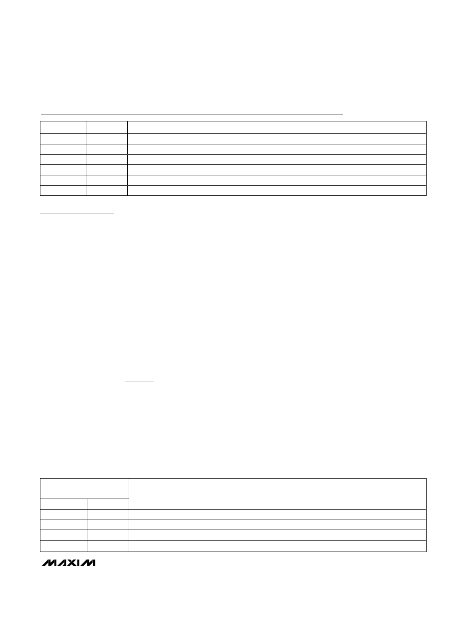
Pin Description
PIN
NAME
FUNCTION
1
V
DD
Power Supply and DAC Reference Input
2
GND
Ground
3
SDA
Bidirectional Serial Data I/O
4
SCL
Serial Clock Line
5
ADD
Address Select. A logic high sets the address LSB to 1; a logic low sets the address LSB to 0.
6
OUT
Analog Output
Table 1. Power-Down Command Bits
POWER-DOWN
COMMAND BITS
PD1
PD0
MODE/FUNCTION
0
0
Power-up device. DAC output restored to previous value.
0
1
Power-down mode 0. Powers down device with output floating.
1
0
Power-down mode 1. Powers down device with output terminated with 1k
Ω to GND.
1
1
Power-down mode 2. Powers down device with output terminated with 100k
Ω to GND.