Table 3. command byte definitions – Rainbow Electronics MAX5812 User Manual
Page 10
MAX5812
12-Bit Low-Power, 2-Wire, Serial
Voltage-Output DAC
10
______________________________________________________________________________________
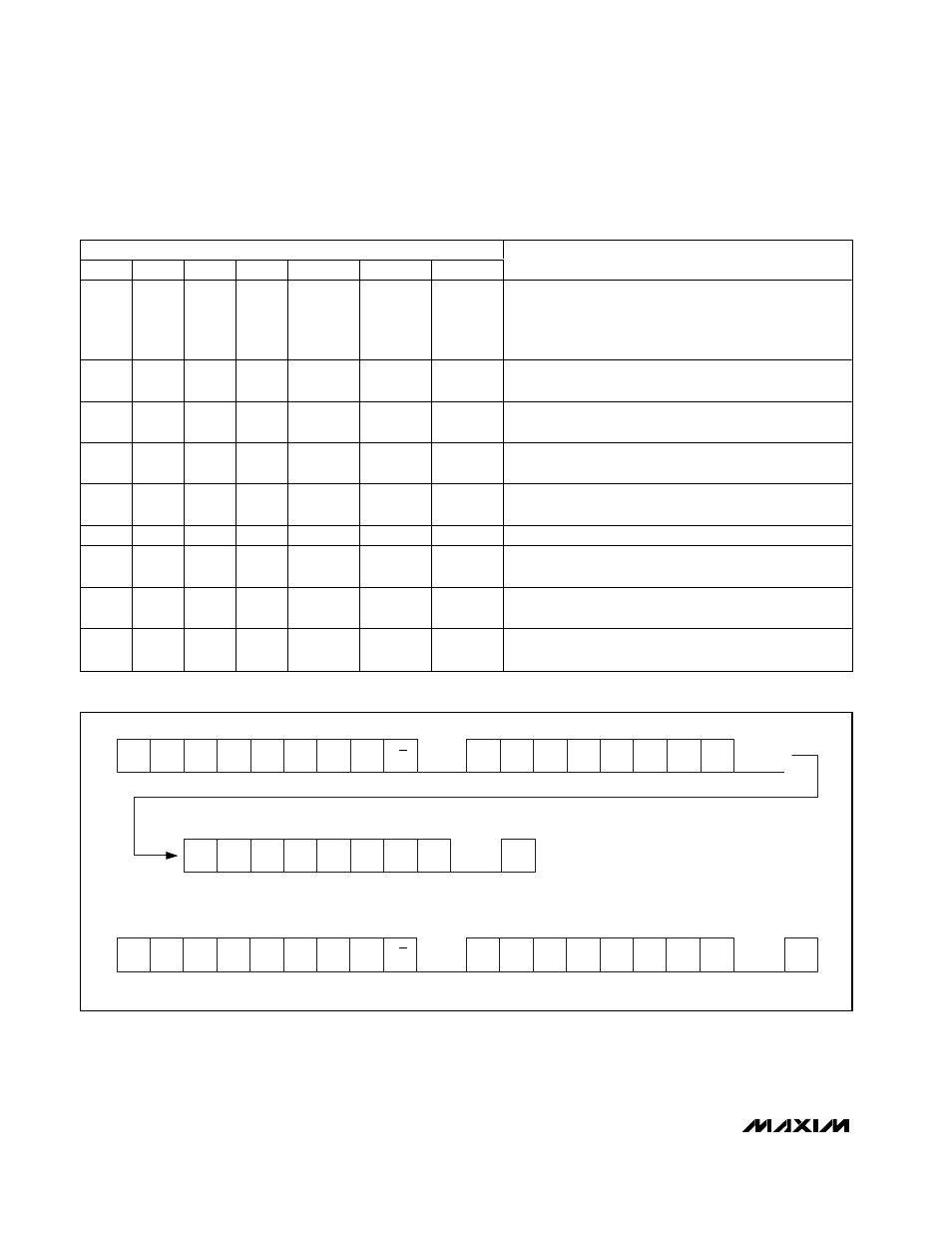
Table 3. Command Byte Definitions
SERIAL DATA INPUT
C3
C2
C1
C0
D11/PD1*
D10/PD0*
D9–D8
FUNCTION
1
1
0
0
DAC
DATA
DAC
DATA
DAC
DATA
Load DAC with a new data from the following data byte
and update DAC output simultaneously as soon as data
is available from the serial bus. The DAC and input
registers are updated with the new data.
1
1
0
1
DAC
DATA
DAC
DATA
DAC
DATA
Load input register with the data from the following data
byte. DAC output remains unchanged.
1
1
1
0
DAC
DATA
DAC
DATA
DAC
DATA
Load input register with data from the following data byte.
Update DAC output to the previously stored data.
1
1
1
1
X
X
XX
Update DAC output from input register. The device will
ignore any new data.
1
0
X
X
X
X
XX
Read data request. Data bits are ignored. The contents of
the DAC register are available on the bus.
0
1
X
X
0
0
XX
Powers up device.
0
1
X
X
0
1
XX
Power-down mode 0. Powers down device with output
floating.
0
1
X
X
1
0
XX
Power-down mode 1. Powers down device with output
terminated with 1k
Ω to GND.
0
1
X
X
1
1
XX
Power-down mode 2. Powers down device with output
terminated with 100k
Ω to GND.
S
MSB
MSB
A6
A5
A4
A3
A2
A1
A0
C3
C2
C1
C0
D11
D10
D9
D8
D7
D6
D5
D4
D3
D2
D1
D0
P
R/W
ACK
ACK
ACK
LSB
MSB
LSB
LSB
S
MSB
A6
A5
A4
A3
A2
A1
A0
C3
C2
X
X
PD1
PD0
X
X
P
R/W
ACK
ACK
LSB
EXAMPLE WRITE DATA SEQUENCE
EXAMPLE WRITE TO POWER-DOWN REGISTER SEQUENCE
MSB
LSB
Figure 6. Example Write Command Sequences
*When C3 = 0 and C2 = 1, data bits D11 and D10 write to the power-down registers (PD1 and PD0).
X = Don’t care.