Applications information – Rainbow Electronics MAX5812 User Manual
Page 11
MAX5812
12-Bit Low-Power, 2-Wire, Serial
Voltage-Output DAC
______________________________________________________________________________________
11
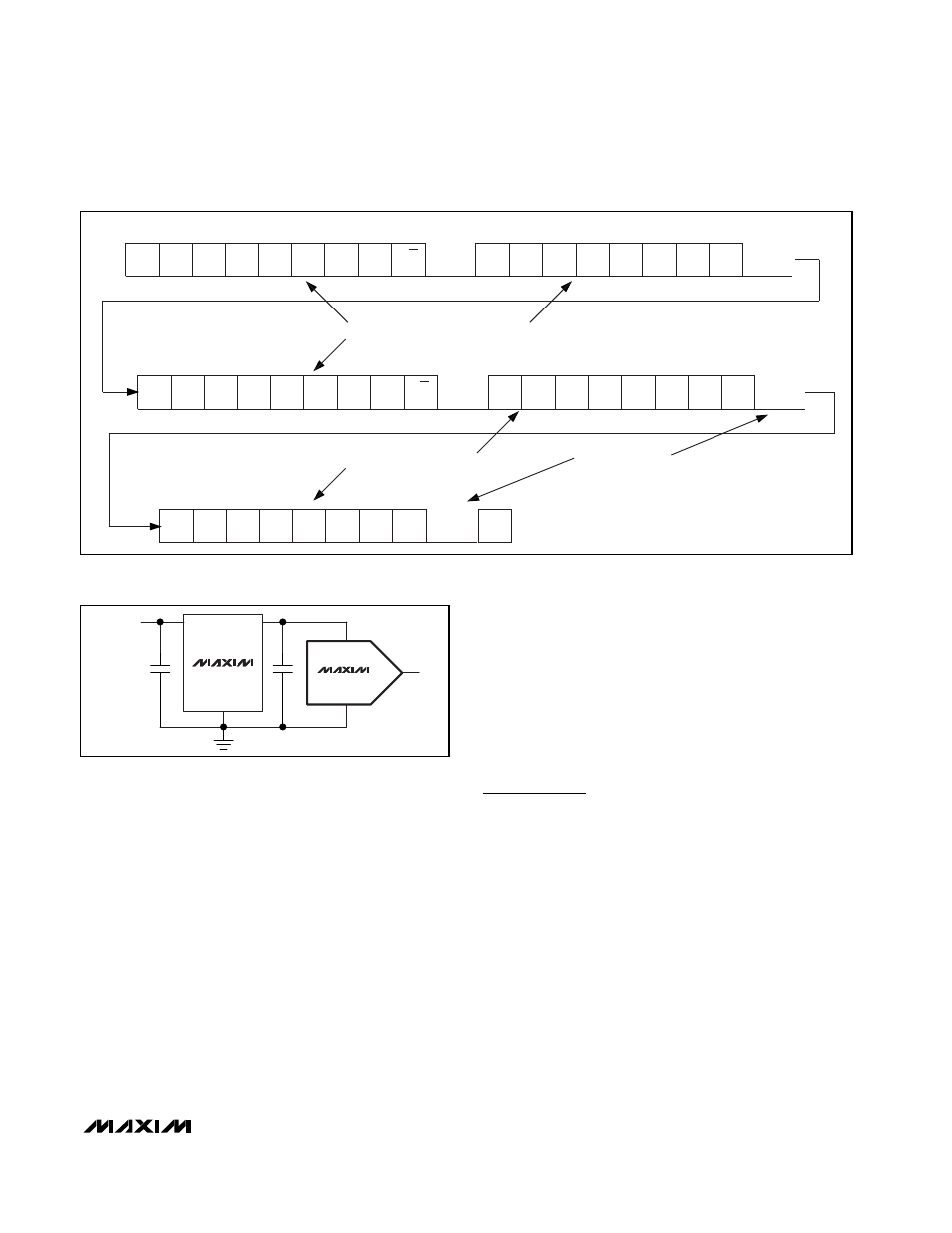
Read Data Format
In read mode (R/W = 1), the MAX5812 writes the con-
tents of the DAC register to the bus. The direction of
data flow reverses after the address acknowledge by
the MAX5812. The device transmits the first byte of
data, waits for the master to acknowledge, and then
transmits the second byte. Figure 7 shows an example-
read data sequence.
I
2
C Compatibility
The MAX5812 is compatible with existing I
2
C systems.
SCL and SDA are high-impedance inputs; SDA has an
open drain that pulls the data line low during the ninth
clock pulse. The Typical Operating Circuit shows a typ-
ical I
2
C application. The communication protocol sup-
ports standard I
2
C 8-bit communications. The general
call address is ignored. The MAX5812 address is com-
patible only with the 7-bit I
2
C addressing protocol. Ten-
bit address formats are not supported.
Digital Feedthrough Suppression
When the MAX5812 detects an address mismatch, the
serial interface disconnects the SCL signal from the
core circuitry. This minimizes digital feedthrough
caused by the SCL signal on a static output. The serial
interface reconnects the SCL signal when a valid
START condition is detected.
Applications Information
Powering the Device From an
External Reference
The MAX5812 uses the V
DD
as the DAC voltage refer-
ence. Any power-supply noise is directly coupled to the
device output. The circuit in Figure 8 uses a precision
voltage reference to power the MAX5812, isolating the
device from any power-supply noise. Powering the
MAX5812 in such a manner greatly improves overall
performance, especially in noisy systems. The
MAX6030 (3V, 75ppm/°C) or the MAX6050 (5V,
75ppm/°C) precision voltage references are ideal
choices because of the low power requirements of the
MAX5812.
Digital Inputs and Interface Logic
The MAX5812 2-wire digital interface is I
2
C and SMBus-
compatible. The two digital inputs (SCL and SDA) load
S
A6
A5
A4
A3
A2
A1
A0
C3
C2
X
X
X
X
X
X
Sr
A6
A5
A4
A3
A2
A1
A0
MSB
LSB
MSB
LSB
LSB
MSB
ACK
ACK
ACK
D7
D6
D5
D4
D3
D2
D1
D0
MSB
LSB
ACK
ACK
P
R/W
= 1
X
X
PD1
PD0
D11
D10
D9
D8
MSB
LSB
DATA BYTES GENERATED BY MASTER DEVICE
DATA BYTES GENERATED BY MAX5812
ACK GENERATED BY
MASTER DEVICE
R/W
= 0
Figure 7. Example Read Word Data Sequence
V
DD
IN
GND
GND
OUT
OUT
MAX5812
MAX6030/
MAX6050
Figure 8. Powering the MAX5812 from An External Reference