Rainbow Electronics MAX8562 User Manual
Page 8
MAX8560/MAX8561/MAX8562
4MHz, 500mA Synchronous Step-Down
DC-DC Converters in SOT and TDFN
8
_______________________________________________________________________________________
Capacitor Selection
Output Capacitor
The output capacitor, C
OUT
, is required to keep the
output voltage ripple small and to ensure regulation
loop stability. C
OUT
must have low impedance at the
switching frequency. Ceramic capacitors with X5R or
X7R dielectrics are highly recommended due to their
small size, low ESR, and small temperature coefficients.
Due to the unique feedback network, the output capac-
itance can be very low. For most applications, a 2.2µF
capacitor is sufficient. For optimum load-transient per-
formance and very low output ripple, the output capaci-
tor value in µFs should be equal to or larger than the
inductor value in µHs.
Input Capacitor
The input capacitor, C
IN
, reduces the current peaks
drawn from the battery or input power source and
reduces switching noise in the IC. The impedance of
C
IN
at the switching frequency should be kept very low.
Ceramic capacitors with X5R or X7R dielectrics are
highly recommended due to their small size, low ESR,
and small temperature coefficients. Due to the
MAX8560/MAX8561/MAX8562s’ soft-start, the input
capacitance can be very low. For most applications, a
2.2µF capacitor is sufficient.
Feed-Forward Capacitor
The feed-forward capacitor, C
FF
, sets the feedback loop
response, controls the switching frequency, and is criti-
cal in obtaining the best efficiency possible. Choose a
small ceramic X7R capacitor with a value given by:
Select the closest standard value to C
FF
as possible.
PC Board Layout and Routing
High switching frequencies and relatively large peak cur-
rents make the PC board layout a very important part of
design. Good design minimizes excessive EMI on the
feedback paths and voltage gradients in the ground
plane, both of which can result in instability or regulation
errors. Connect C
IN
as close as possible to IN and GND.
Connect the inductor and output capacitor as close to
the IC as possible and keep their traces short, direct,
and wide. Connect GND and PGND separately to the
ground plane. The external feedback network should be
very close to the FB pin, within 0.2in (5mm). Keep noisy
traces, such as the LX node, as short as possible. For
the 8-pin TDFN package, connect GND to the exposed
paddle directly under the IC. Figure 4 illustrates an
example PC board layout and routing scheme.
C
L
R
Siemens
FF
=
×
1
10
GND
IN
LX
FB
ODO
PGND
ODI
SHDN
ON/OFF
OUTPUT
1.5V OR 1.0V
AT 500mA
INPUT
Li+ BATTERY
2.2
µH
2.2
µF
2.2
µF
220pF
100k
Ω
120k
Ω
150k
Ω
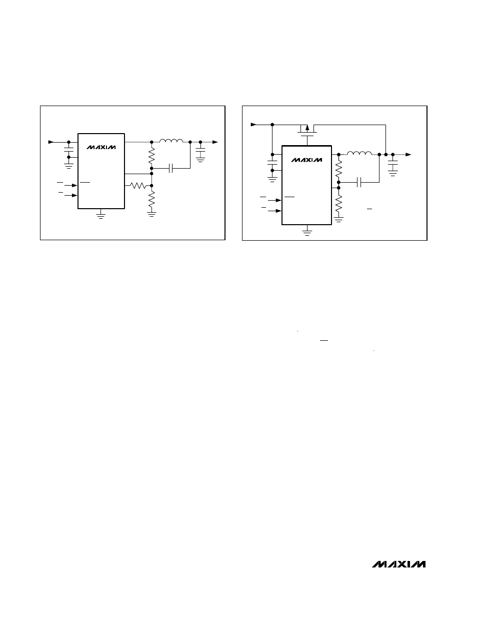
MAX8561
1.5/1.0
Figure 2. Using ODI/ODO to Obtain Two Output Voltages from
the MAX8561
GND
PFET
IN
LX
FB
ODO
ODI
SHDN
ON/OFF
OUTPUT
1.2V OR V
BATT
1.5
µH
2.2
µF
2.2
µF
150pF
100k
Ω
100k
Ω
HP = HIGH-POWER MODE
LP = LOW-POWER MODE
MAX8562
INPUT
Li+ BATTERY
HP/LP
PGND
Figure 3. Using the MAX8562 to Control an External Bypass
PFET for a Two-Step V
CC
in CDMA-PA Applications