Absolute maximum ratings, Electrical characteristics – Rainbow Electronics MAX8562 User Manual
Page 2
MAX8560/MAX8561/MAX8562
4MHz, 500mA Synchronous Step-Down
DC-DC Converters in SOT and TDFN
2
_______________________________________________________________________________________
ABSOLUTE MAXIMUM RATINGS
Stresses beyond those listed under “Absolute Maximum Ratings” may cause permanent damage to the device. These are stress ratings only, and functional
operation of the device at these or any other conditions beyond those indicated in the operational sections of the specifications is not implied. Exposure to
absolute maximum rating conditions for extended periods may affect device reliability.
IN, FB, SHDN, ODI, ODO to GND ............................-0.3V to +6V
LX to GND (Note 1)......................................-0.3V to (V
IN
+ 0.3V)
PGND to GND .......................................................-0.3V to +0.3V
LX Current ...........................................................................1.27A
Output Short Circuit to GND
(typical operating circuit)....................................................10s
Continuous Power Dissipation (T
A
= +70°C)
6-Pin SOT23 (derate 8.7mW/°C above +70°C)............695mW
8-Pin TDFN (derate 24.4mW/°C above +70°C) .........1951mW
Operating Temperature Range ...........................-40°C to +85°C
Junction Temperature ......................................................+150°C
Storage Temperature Range .............................-65°C to +150°C
Lead Temperature (soldering, 10s) .................................+300°C
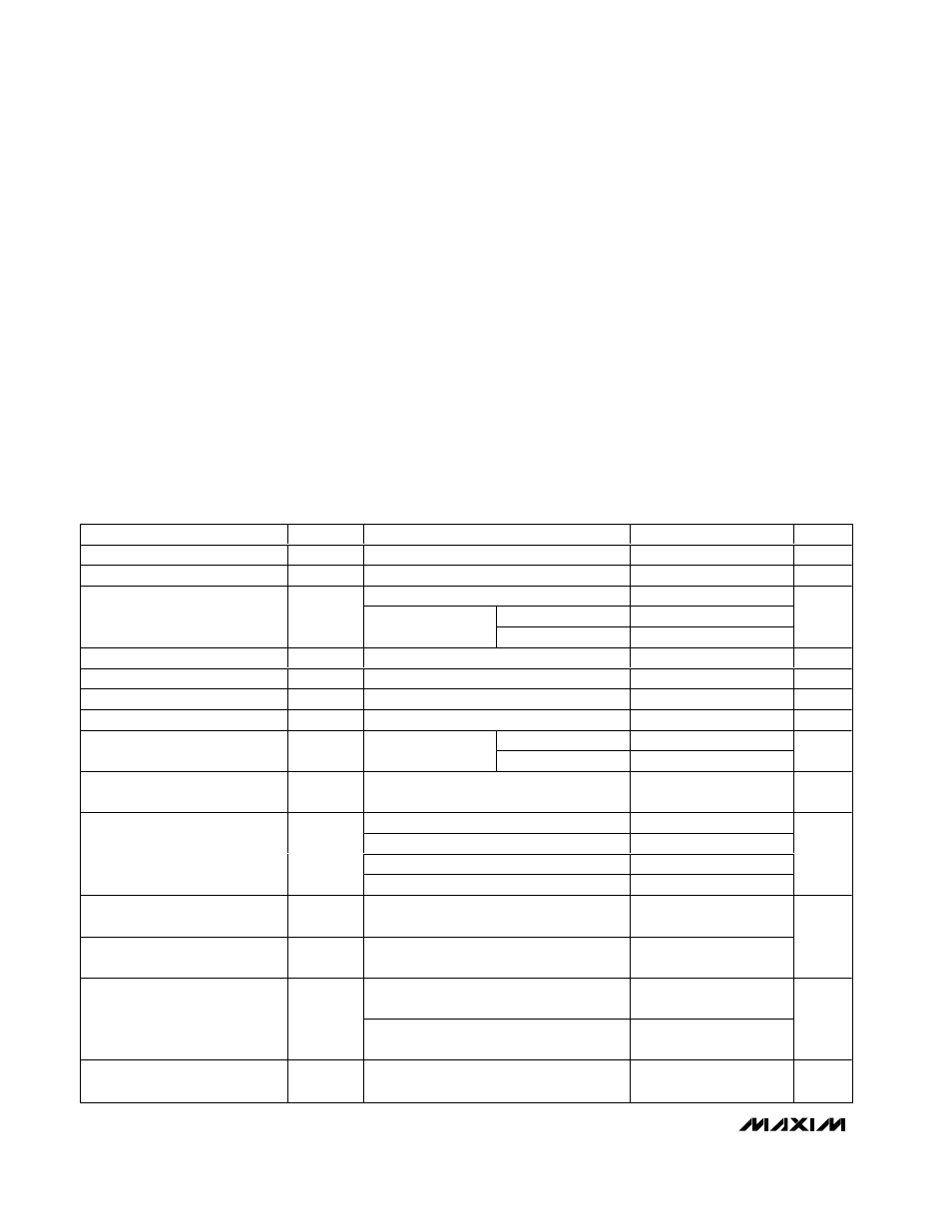
ELECTRICAL CHARACTERISTICS
(V
IN
= 3.6V, SHDN = IN, T
A
= -40°C to +85°C, typical values are at T
A
= +25°C, unless otherwise noted.) (Note 1)
PARAMETER
SYMBOL
CONDITIONS
MIN
TYP
MAX
UNITS
Supply Voltage Range
V
IN
2.7
5.5
V
UVLO Threshold
UVLO
V
IN
rising, 60mV hysteresis
2.4
2.5
2.6
V
I
LOAD
= 0mA, no switching
40
80
T
A
= +25°C
0.01
0.1
Supply Current
I
IN
SHDN = GND
T
A
= +85°C
0.1
µA
Output Voltage Range
V
OUT
0.6
2.5
V
FB Threshold Voltage
V
FB
V
FB
falling
0.6
V
FB Threshold Line Regulation
V
IN
= 2.7V to 5.5V
0.3
% / V
FB Threshold Load Regulation
I
OUT
= 0 to 500mA
-0.001
%/mA
T
A
= +25°C
-1.5
+1.5
FB Threshold Voltage Accuracy
(Falling) (% of V
FB
)
I
LOAD
= 0mA
T
A
= -40°C to +85°C
-2.5
+2.5
%
%
FB Threshold Voltage Hysteresis
(% of V
FB
)
V
HYS
1.0
%
SHDN = GND, T
A
= +25°C, V
IN
= 5.5V
0.01
0.1
SHDN = GND, T
A
= +85°C, V
IN
= 5.5V
0.1
V
FB
= 0.5V, T
A
= +25°C, V
IN
= 5.5V
0.01
0.1
FB Bias Current
I
FB
V
FB
= 0.5V, T
A
= +85°C, V
IN
= 5.5V
0.1
µA
Logic Input High Voltage
(
SHDN, ODI)
V
IH
V
IN
= 2.7V to 5.5V
1.41
Logic Input Low Voltage
(
SHDN, ODI)
V
IL
V
IN
= 2.7V to 5.5V
0.4
V
V
IN
= 5.5V,
SHDN = ODI = GND or IN,
T
A
= +25°C
0.001
0.1
Logic Input Bias Current
I
IH
, I
IL
V
IN
= 5.5V,
SHDN = ODI = GND or IN,
T
A
= +85°C
0.01
µA
ODO Output Low Voltage
(MAX8562 Only)
V
OL
1mA sink current, V
IN
= 2.7V
0.02
0.1
V
Note 1: LX has internal clamp diodes to PGND and IN. Applications that forward bias these diodes should take care not to exceed
the IC’s package power-dissipation limits.