Table 2. gain settings – Rainbow Electronics MAX9714 User Manual
Page 10

MAX9713/MAX9714
In the class D case, an 8mV offset into 8
Ω equates
to an additional power drain of 8µW. Due to the high
efficiency of the class D amplifier, this represents an
additional quiescent current draw of: 8µW/(V
DD
/100
✕
η),
which is on the order of a few microamps.
Input Amplifier
Differential Input
The MAX9713/MAX9714 feature a differential input struc-
ture, making them compatible with many CODECs, and
offering improved noise immunity over a single-ended
input amplifier. In devices such as PCs, noisy digital sig-
nals can be picked up by the amplifier’s input traces.
The signals appear at the amplifiers’ inputs as common-
mode noise. A differential input amplifier amplifies the
difference of the two inputs, any signal common to both
inputs is canceled.
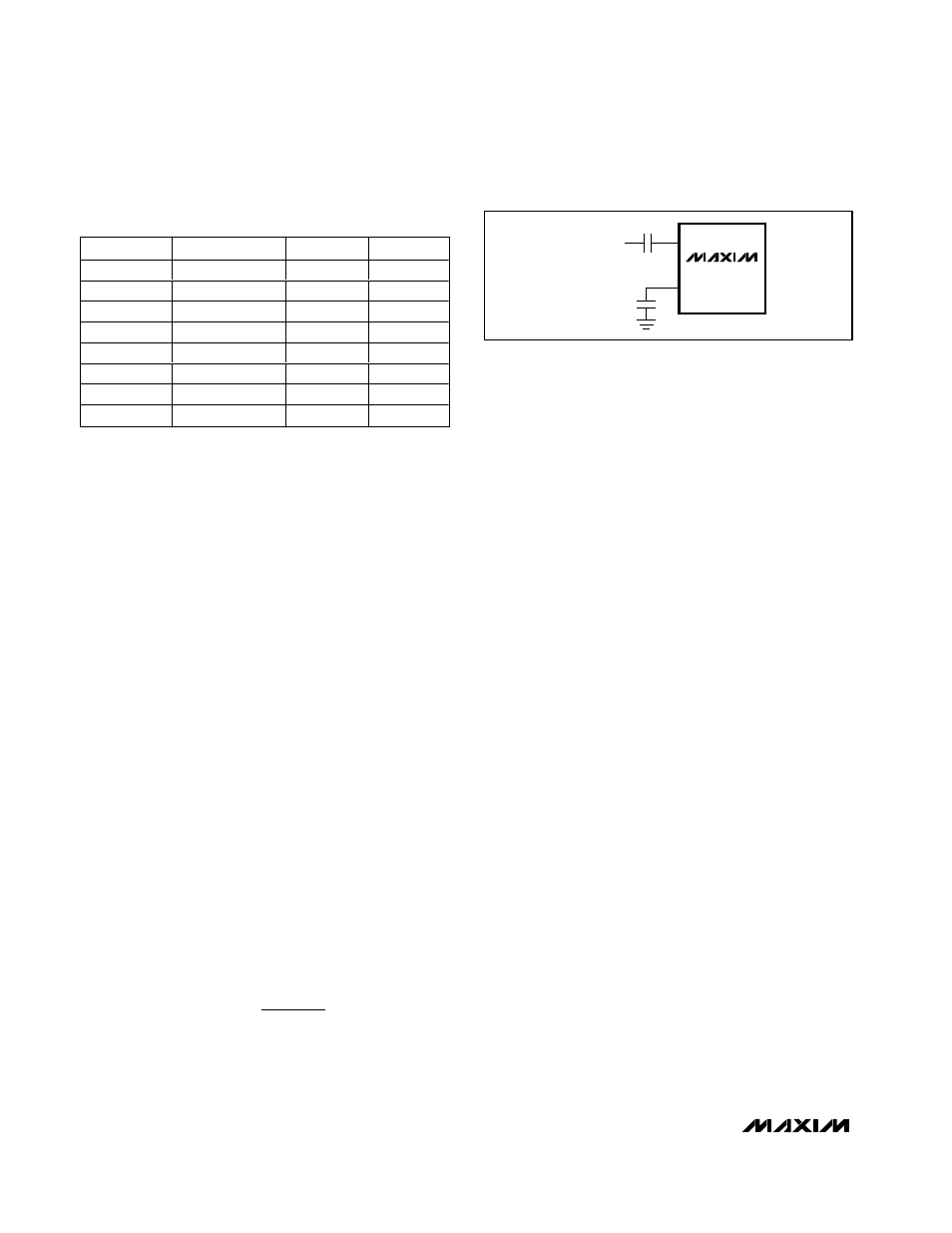
Single-Ended Input
The MAX9713/MAX9714 can be configured as single-
ended input amplifiers by capacitively coupling either
input to GND and driving the other input (
Figure 4
).
Component Selection
Input Filter
An input capacitor, C
IN
, in conjunction with the input
impedance of the MAX9713/MAX9714, forms a high-
pass filter that removes the DC bias from an incoming
signal. The AC-coupling capacitor allows the amplifier
to bias the signal to an optimum DC level. Assuming
zero-source impedance, the -3dB point of the highpass
filter is given by:
Choose C
IN
so f
-3dB
is well below the lowest frequency
of interest. Setting f
-3dB
too high affects the low-fre-
quency response of the amplifier. Use capacitors
whose dielectrics have low-voltage coefficients, such
as tantalum or aluminum electrolytic. Capacitors with
high-voltage coefficients, such as ceramics, may result
in increased distortion at low frequencies.
Charge-Pump Capacitor Selection
Use capacitors with an ESR less than 100m
Ω for opti-
mum performance. Low-ESR ceramic capacitors mini-
mize the output resistance of the charge pump. For
best performance over the extended temperature
range, select capacitors with an X7R dielectric.
Flying Capacitor (C1)
The value of the flying capacitor (C1) affects the load
regulation and output resistance of the charge pump. A
C1 value that is too small degrades the device’s ability to
provide sufficient current drive. Increasing the value of
C1 improves load regulation and reduces the charge-
pump output resistance to an extent. Above 1µF, the on-
resistance of the switches and the ESR of C1 and C2
dominate.
Output Capacitor (C2)
The output capacitor value and ESR directly affect the
ripple at CHOLD. Increasing C2 reduces output ripple.
Likewise, decreasing the ESR of C2 reduces both rip-
ple and output resistance. Lower capacitance values
can be used in systems with low maximum output
power levels.
Output Filter
The MAX9713/MAX9714 do not require an output filter.
The device passes FCC emissions standards with
36cm of unshielded speaker cables. However, output
filtering can be used if a design is failing radiated emis-
sions due to board layout or cable length, or the circuit
is near EMI-sensitive devices. Use a ferrite bead filter
when radiated frequencies above 10MHz are of con-
cern. Use an LC filter when radiated frequencies below
10MHz are of concern, or when long leads connect the
amplifier to the speaker. Refer to the MAX9714
Evaluation Kit schematic for details of this filter.
f
R C
-3dB
IN IN
1
2
=
π
6W, Filterless, Spread-Spectrum
Mono/Stereo Class D Amplifiers
10
______________________________________________________________________________________
Table 2. Gain Settings
GAIN (dB)
INPUT (V
RMS
)
R
L
(
Ω)
P
OUT
(W)
13.0
1.79
16
8
16.1
1.25
16
8
19.1
0.89
16
8
22.1
1.79
16
8
13.0
1.10
8
6
16.1
0.77
8
6
19.1
0.54
8
6
22.1
0.38
8
6
MAX9713/
MAX9714
IN+
IN-
0.47
µF
0.47
µF
SINGLE-ENDED
AUDIO INPUT
Figure 4. Single-Ended Input
