Chip information, Table 8. conversion-rate control byte – Rainbow Electronics MAX6681 User Manual
Page 15
reside on the same bus without address conflicts
(Table 9).
The address pin states are checked at POR and RESET
only, and the address data stays latched to reduce qui-
escent supply current due to the bias current needed
for high-Z state detection. The MAX6680/MAX6681 also
respond to the SMBus Alert Response slave address
(see the Alert Response Address section).
POR and UVLO
The MAX6680/MAX6681 have a volatile memory. To
prevent unreliable power-supply conditions from cor-
rupting the data in memory and causing erratic behav-
ior, a POR voltage detector monitors V
CC
and clears the
memory if V
CC
falls below 1.91V (typ, see Electrical
Characteristics). When power is first applied and V
CC
rises above 2.0V (typ), the logic blocks begin operating,
although reads and writes at V
CC
levels below 3.0V are
not recommended. A second V
CC
comparator, the ADC
UVLO comparator, prevents the ADC from converting
until there is sufficient headroom (V
CC
= 2.8V typ).
Power-Up Defaults
• Interrupt latch is cleared.
• Address select pin is sampled.
• ADC begins autoconverting at a 1Hz rate (legacy
resolution).
• Command register is set to 00h to facilitate quick
internal Receive Byte queries.
• T
HIGH
and T
LOW
registers are set to max and min
limits, respectively.
• Hysteresis is set to 6°C.
• Transistor type is set to a substrate or common-col-
lector PNP.
Temperature Offset
The MAX6680/MAX6681 are designed to provide ±1°C
accuracy for common microprocessors and discrete
transistors. To accommodate processes that differ sig-
nificantly in their ideality factor, the user can
increase/decrease the Remote Temperature Sensor
Data register with an offset by writing to the External
Offset High and Low Byte registers (11h and 12h,
respectively). The offset temperature data is represent-
ed as a 10 bits + sign with a 0.125LSB resolution.
MAX6680/MAX6681
±1°C Fail-Safe Remote/Local Temperature
Sensors with SMBus Interface
______________________________________________________________________________________
15
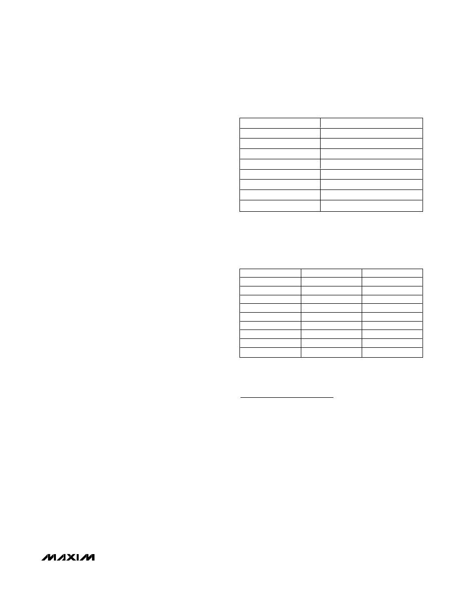
DATA
CONVERSION RATE (Hz)
00h
0.0625
01h
0.125
02h
0.25
03h
0.5
04h
1
05h
2
06h
4
07h
8
Table 8. Conversion-Rate Control Byte
Note: If extended resolution is selected using bit 4 of the
Configuration register, the extended conversion is limited to a
maximum of 4Hz.
ADD0
ADD1
ADDRESS
GND
GND
0011 000
GND
HIGH-Z
0011 001
GND
V
CC
0011 010
HIGH-Z
GND
0101 001
HIGH-Z
HIGH-Z
0101 010
HIGH-Z
V
CC
0101 011
V
CC
GND
1001 100
V
CC
HIGH-Z
1001 101
V
CC
V
CC
1001 110
Table 9. POR Slave Address Decoding
(ADD0 and ADD1)
Chip Information
TRANSISTOR COUNT: 17,150
PROCESS: BiCMOS