Chip information, Pin configurations (continued) – Rainbow Electronics MAX9077 User Manual
Page 7
4) Choose the threshold voltage for V
IN
rising (V
THR
). In
this example, choose V
THR
= 3V.
5) Calculate R2 as follows:
R2 = 1 / {[V
THR
/ (V
REF
✕
R1)] - 1/R1 - 1/R3} =
1 / {[3 / (1.2
✕
100k
Ω)] - 1/100kΩ - 1/10MΩ} = 67.114kΩ
A 1% preferred value is 64.9k
Ω.
6) Verify the threshold voltages with these formulas:
V
IN
rising:
V
THR
= V
REF
✕
R1 (1/R1 + 1/R2 + 1/R3)
V
IN
falling:
V
THF
= V
THR
- (R1
✕
V
CC
) / R3
7) Check the error due to input bias current (5nA). If the
error is too large, reduce R3 and recalculate.
V
TH
= I
B
(R1
✕
R2
✕
R3) / (R1 + R2 + R3) = 0.2mV
Board Layout and Bypassing
Use 10nF power-supply bypass capacitors. Use 100nF
bypass capacitors when supply impedance is high,
when supply leads are long, or when excessive noise is
expected on the supply lines. Minimize signal trace
lengths to reduce stray capacitance. Minimize the
capacitive coupling between IN- and OUT. For slow-
moving input signals (rise time > 1ms) use a 1nF
capacitor between IN+ and IN-.
Chip Information
MAX9075 TRANSISTOR COUNT: 86
MAX9077 TRANSISTOR COUNT: 142
MAX9075/MAX9077
Low-Cost, Ultra-Small, 3µA
Single-Supply Comparators
_______________________________________________________________________________________
7
V
CC
V
IN
V
CC
OUT
GND
V
REF
R3
R2
R1
MAX9075
MAX9077
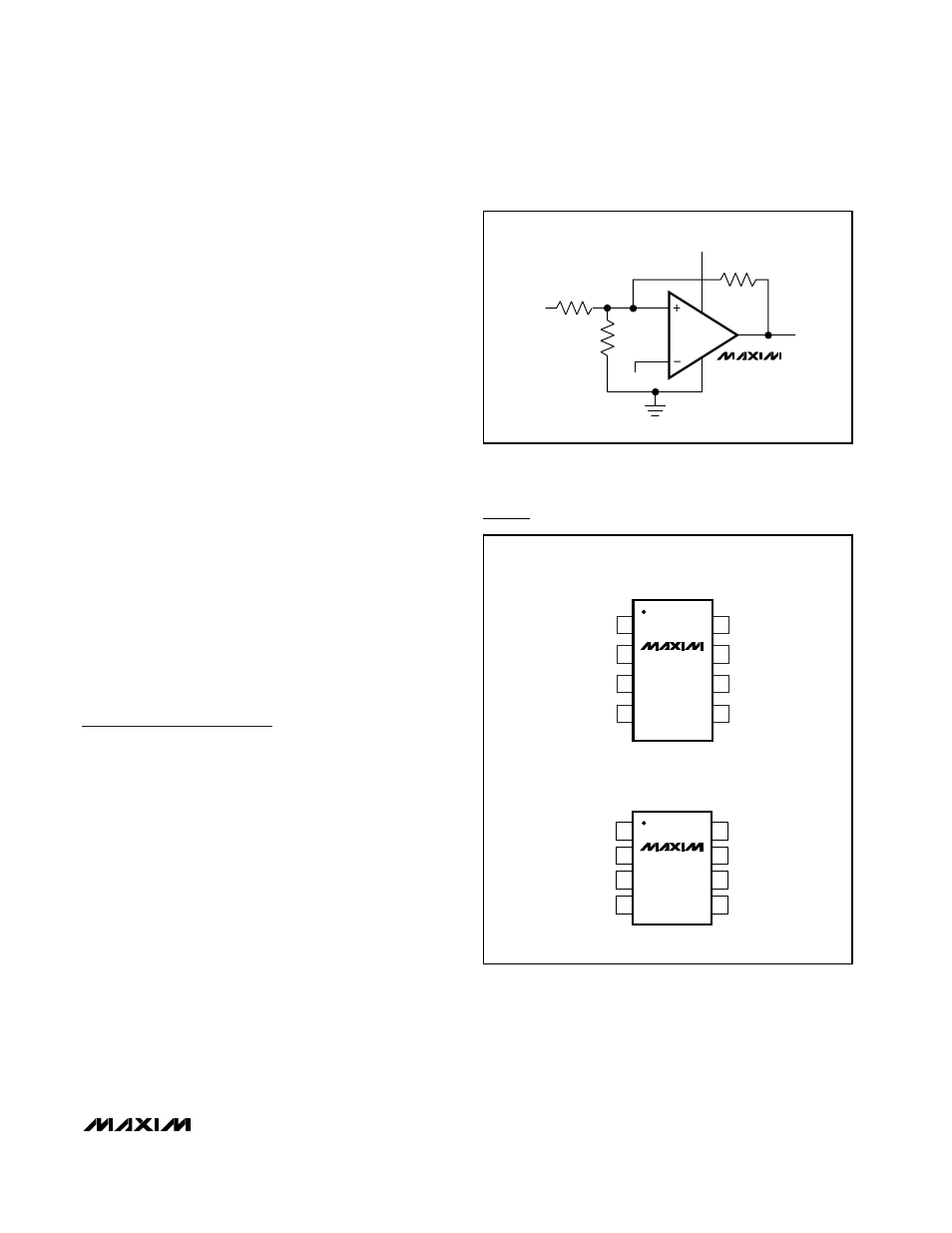
Figure 1. Adding Hysteresis
INB-
INB+
INA+
1
2
8
7
V
CC
OUTB
GND
INA-
OUTA
SOT23-8
TOP VIEW
3
4
6
5
INB-
INB+
GND
1
2
8
7
V
CC
OUTB
INA-
INA+
OUTA
µMAX/SO
3
4
6
5
MAX9077
MAX9077
Pin Configurations (continued)