Rainbow Electronics MAX9077 User Manual
Page 2
V
CC
= 5V
MAX9075/MAX9077
Low-Cost, Ultra-Small, 3µA
Single-Supply Comparators
2
_______________________________________________________________________________________
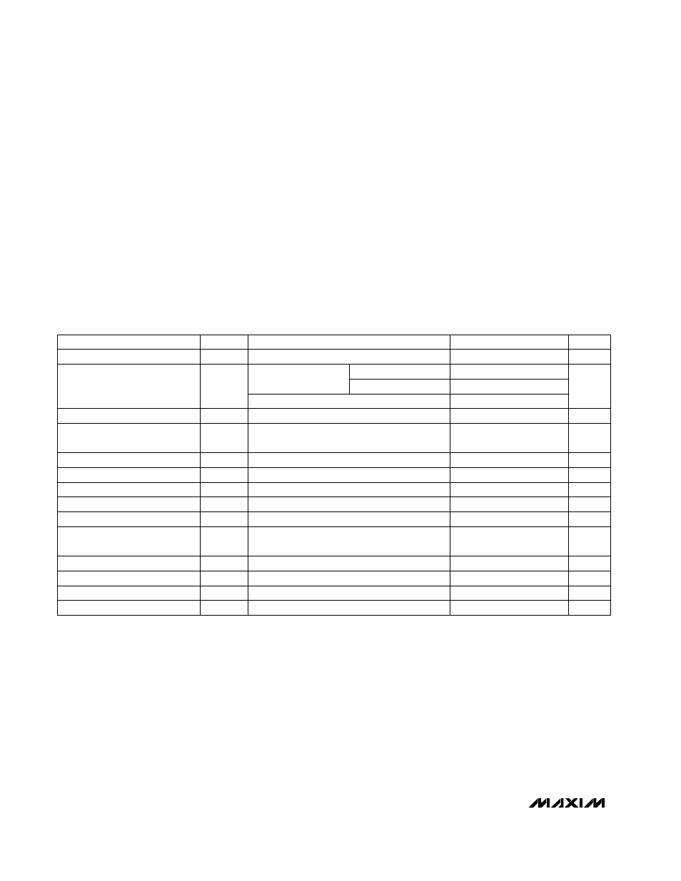
ABSOLUTE MAXIMUM RATINGS
ELECTRICAL CHARACTERISTICS
(V
CC
= 5V, V
CM
= -0.2V, T
A
= T
MIN
to T
MAX
, unless otherwise noted. Typical values are at T
A
= +25°C.) (Note 1)
Stresses beyond those listed under “Absolute Maximum Ratings” may cause permanent damage to the device. These are stress ratings only, and functional
operation of the device at these or any other conditions beyond those indicated in the operational sections of the specifications is not implied. Exposure to
absolute maximum rating conditions for extended periods may affect device reliability.
Note 1: All devices are 100% production tested at T
A
= +25°C. All temperature limits are guaranteed by design.
Note 2: Inferred from CMRR. Either input can be driven to the absolute maximum limit without output inversion, as long as the other
input is within the input voltage range.
Note 3: Guaranteed by design.
Supply Voltage
V
CC
to GND........................................................................6V
All Other Pins to GND...........................-0.3V to (V
CC
+ 0.3V)
Duration of Output Short-Circuit to GND or V
CC
........Continuous
Continuous Power Dissipation (T
A
= +70°C)
5-Pin SC70 (derate 2.5mW/°C above +70°C) ............200mW
5-Pin SOT23 (derate 7.1mW/°C above +70°C)..........571mW
8-Pin SOT23 (derate 5.3mW/°C above +70°C)..........421mW
8-Pin µMAX (derate 4.5mW/°C above +70°C) ...........362mW
8-Pin SO (derate 5.88mW/°C above +70°C)..............471mW
Operating Temperature Range ...........................-40°C to +85°C
Storage Temperature Range .............................-65°C to +150°C
Lead Temperature (soldering, 10s) .................................+300°C
Inferred from PSRR
C
LOAD
= 10pF
-0.2V
≤ V
CM
≤ (V
CC
- 1.2V)
C
LOAD
= 10pF, overdrive = 100mV
C
LOAD
= 10pF, overdrive = 100mV
V
CM
= 0 (Note 3)
V
CC
= 3V
2.1V
≤ V
CC
≤ 5.5V
(Note 2)
I
SINK
= 2mA
I
SOURCE
= 2mA
CONDITIONS
ns
1.6
Rise/Fall Time
ns
250
t
PD-
Propagation Delay High to Low
ns
580
t
PD+
Propagation Delay Low to High
V
0.4
V
OL
OUT_ Output Voltage Low
V
V
CC
-
0.4
V
OH
OUT_ Output Voltage High
6.6
3
5.2
I
CC
V
2.1
5.5
V
CC
Operating Supply Voltage Range
Supply Current per Comparator
dB
60
82
CMRR
Common-Mode Rejection Ratio
pF
3
C
IN
Input Capacitance
nA
-5
-20
I
B
Input Bias Current
nA
1
I
OS
Input Offset Current
2.4
dB
54
77
PSRR
Power-Supply Rejection Ratio
V
-0.2
V
CC
-
1.2
V
CMR
Common-Mode Voltage Range
mV
±1
±8
V
OS
Input Offset Voltage
UNITS
MIN
TYP
MAX
SYMBOL
PARAMETER
T
A
= +25°C
T
A
= T
MIN
to T
MAX
V
CC
= 5V
µA