Pin description, Detailed description, Applications information – Rainbow Electronics MAX9077 User Manual
Page 6
MAX9075/MAX9077
Low-Cost, Ultra-Small, 3µA
Single-Supply Comparators
6
_______________________________________________________________________________________
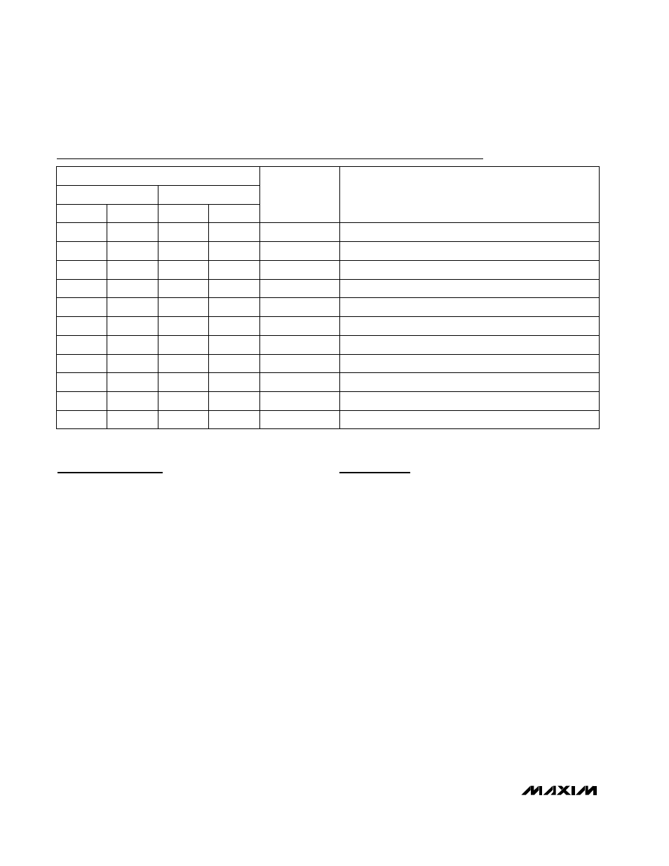
Pin Description
FUNCTION
NAME
SOT23
MAX9077
µMAX/SO
SC70
SOT23
—
1
—
Comparator Output
OUT
1
1
—
1
4
2
2
Ground
GND
2
Output of Comparator A
OUTA
—
—
3
—
3
—
4
Noninverting Input of Comparator A
INA+
—
—
4
—
2
—
3
Inverting Input of Comparator A
INA-
—
Inverting Comparator Input
IN-
4
Noninverting Comparator Input
IN+
3
8
5
8
Positive Supply Voltage
V
CC
5
5
—
5
6
—
6
Inverting Input of Comparator B
INB-
—
7
—
7
Output of Comparator B
OUTB
—
Noninverting Input of Comparator B
INB+
—
MAX9075
PIN
Detailed Description
The MAX9075/MAX9077 feature a 580ns propagation
delay from an ultra-low supply current of only 3µA per
comparator. These devices are capable of single-sup-
ply operation in the 2.1V to 5.5V range. Large internal
output drivers allow rail-to-rail output swing with up to
2mA loads. Both comparators offer a push-pull output
that sinks and sources current.
Comparator Output
The MAX9075/MAX9077 are designed to maintain a
low-supply current during repeated transitions by limit-
ing the shoot-through current.
Noise Considerations, Comparator Input
The input common-mode voltage range for these
devices extends from -0.2V to V
CC
- 1.2V. Unlike many
other comparators, the MAX9075/MAX9077 can oper-
ate at any differential input voltage within these limits.
Input bias current is typically -5nA if the input voltage is
between the supply rails.
Although the comparators have a very high gain, useful
gain is limited by noise. The comparator has a wide-
band peak-to-peak noise of approximately 70µV.
Applications Information
Adding Hysteresis
Hysteresis extends the comparator’s noise margin by
increasing the upper threshold and decreasing the
lower threshold. A voltage divider from the output of the
comparator sets the trip voltage. Therefore, the trip
voltage is related to the output voltage. Set the hystere-
sis with three resistors using positive feedback, as
shown in Figure 1.
The design procedure is as follows:
1) Choose R3. The leakage current of IN+ may cause a
small error; however, the current through R3 can be
approximately 500nA and still maintain accuracy.
The added supply current due to the circuit at the
trip point is V
CC
/R3; 10M
Ω is a good practical value
for R3, as this keeps the current well below the sup-
ply current of the chip.
2) Choose the hysteresis voltage (V
HYS
), which is the
voltage between the upper and lower thresholds. In
this example, choose V
HYS
= 50mV and assume
V
REF
= 1.2V and V
CC
= 5V.
3) Calculate R1 as follows:
R1 = R3 · V
HYS
/ V
CC
= 10M
Ω · 0.05 / 5 = 100kΩ