Table 3. detailed sspcon register contents, Table 4. detailed sspstat register contents – Rainbow Electronics MAX5121 User Manual
Page 13

Serial Data Output
The contents of the internal shift register are output
serially on DOUT, which allows for daisy-chaining (see
Applications Information
) of multiple devices as well as
data readback. The MAX5120/MAX5121 may be pro-
grammed to shift data out on DOUT on the serial
clock’s rising edge (Mode 1) or falling edge (Mode 0).
The latter is the default during power-up and provides a
lag of 16 clock cycles, maintaining SPI, QSPI,
MICROWIRE, and PIC16/PIC17 compatibility. In Mode
1, the output data lags DIN by 15.5 clock cycles.
During power-down, DOUT retains its last digital state
prior to shutdown.
User-Programmable Output (UPO)
The UPO feature allows an external device to be con-
trolled through the serial-interface setup (Table 1),
thereby reducing the number of microcontroller I/O
ports required. During power-down, this output will
retain the last digital state before shutdown. With CLR
pulled low, UPO will reset to the default state after wake
up.
MAX5120/MAX5121
+3V/+5V, 12-Bit, Serial Voltage-Output DACs
with Internal Reference
______________________________________________________________________________________
13
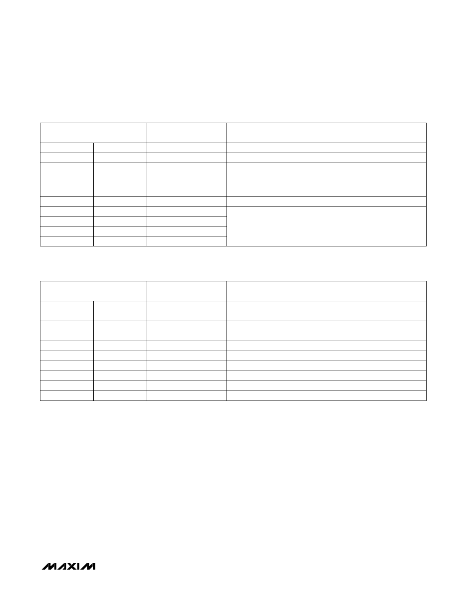
Table 3. Detailed SSPCON Register Contents
Receive Overflow Detection Bit
X
SSPOV
BIT6
BIT7
Clock Polarity Select Bit. CKP = 0 for SPI master-mode selection.
0
CKP
BIT4
BIT5
Synchronous Serial Port Enable Bit.
0: Disables serial port and configures these pins as I/O port pins.
1: Enables serial port and configures SCK, SDO, and SCI as serial-
port pins.
1
SSPEN
0
SSPM2
BIT2
BIT3
1
SSPM0
BIT0
BIT1
CONTROL BIT
0
SSPM1
Write Collision Detection Bit
X
WCOL
SYNCHRONOUS SERIAL-PORT CONTROL REGISTER
(SSPCON)
MAX5120/MAX5121
SETTINGS
Synchronous Serial Port Mode Select Bit. Sets SPI master mode
and selects f
CLK
= f
OSC
/ 16.
0
SSPM3
X
= Don’t care
Table 4. Detailed SSPSTAT Register Contents
X
= Don’t care
SPI Clock Edge Select Bit. Data will be transmitted on the rising
edge of the serial clock.
1
CKE
BIT6
Buffer Full Status Bit
BIT7
Update Address
Read/Write Bit Information
Stop Bit
X
P
BIT4
BIT5
Data Address Bit
X
D/A
X
R/W
BIT2
BIT3
X
BF
BIT0
BIT1
CONTROL BIT
X
UA
SPI Data Input Sample Phase. Input data is sampled at the mid-
dle of the data output time.
0
SMP
SYNCHRONOUS SERIAL-PORT CONTROL REGISTER
(SSPSTAT)
MAX5120/MAX5121
SETTINGS
Start Bit
X
S
