Table 2. serial data format, Pic16 with ssp module and pic17 interface – Rainbow Electronics MAX5121 User Manual
Page 12
MAX5120/MAX5121
The 16-bit input word may be sent in two 1-byte pack-
ets (SPI-, MICROWIRE- and PIC16/PIC17-compatible),
with CS low during this period. The control bits C2, C1,
and C0 (Table 1) determine:
•
The clock edge on which DOUT is to be clocked out
via the serial interface;
•
The state of the user-programmable logic output;
•
The configuration of the device after shutdown.
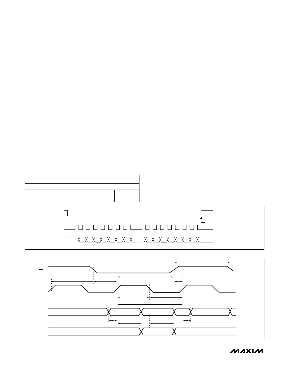
The general timing diagram in Figure 6 illustrates how
data is acquired. CS must be low for the part to receive
data. With CS low, data at DIN is clocked into the regis-
ter on the rising edge of SCLK. When CS transitions
high, data is latched into the input and/or DAC registers,
depending on the setting of the three control bits C2,
C1, and C0. The maximum serial clock frequency guar-
anteed for proper operation is 10MHz for the MAX5120
and 6.6MHz for the MAX5121. Figure 7 depicts a more
detailed timing diagram of the serial interface.
Table 2. Serial Data Format
PIC16 with SSP Module and
PIC17 Interface
The MAX5120/MAX5121 are compatible with a PIC16/
PIC17 controller (µC), using the synchronous serial port
(SSP) module. To establish SPI communication connect
the controller as shown in Figure 4 and configure the
PIC16/PIC17 as system master by initializing its syn-
chronous serial port control register (SSPCON) and
synchronous serial port status register (SSPSTAT) to
the bit patterns shown in Tables 3 and 4.
In SPI mode, the PIC16/PIC17 µCs allow 8 bits of data
to be transmitted synchronously and received simulta-
neously. Two consecutive 8-bit writings (Figure 6) are
necessary to feed the DAC with three control bits and
12 data bits plus one sub-bit. DIN data transitions on
the serial clock’s falling edge and is clocked into the
DAC on SCLK’s rising edge. The first 8 bits on DIN con-
tain the 3 control bits (C2, C1, and C0) and the first five
data bits (D11–D7). The second 8-bit word contains the
remaining bits (D6–D0), and the sub-bit S0.
+3V/+5V, 12-Bit, Serial Voltage-Output DACs
with Internal Reference
12
______________________________________________________________________________________
Control Bits
MSB .... Data Bits ..... LSB
MSB ............................................................................... LSB
⇐
16 BITS OF SERIAL DATA
⇒
D11................................D0
C2, C1, C0
CS
SCLK
DIN
COMMAND
EXECUTED
9
8
16
1
C1
C2
S0
C0
D11 D10
D9
D8
D5
D4
D3
D2
D1
D0
D7
D6
Figure 6. Serial-Interface Timing
SCLK
DIN
DOUT
t
CS0
t
CSS
t
CL
t
CH
t
CP
t
CSW
t
CS1
t
CSH
t
DS
t
DO1
t
DO2
t
DH
CS
Figure 7. Detailed Serial-Interface Timing
S0
Sub-Bit