3 schematic, Qt5480, Figure 1-1. typical circuit – Rainbow Electronics AT42QT5480 User Manual
Page 5
5
9510AS–AT42–10/08
QT5480
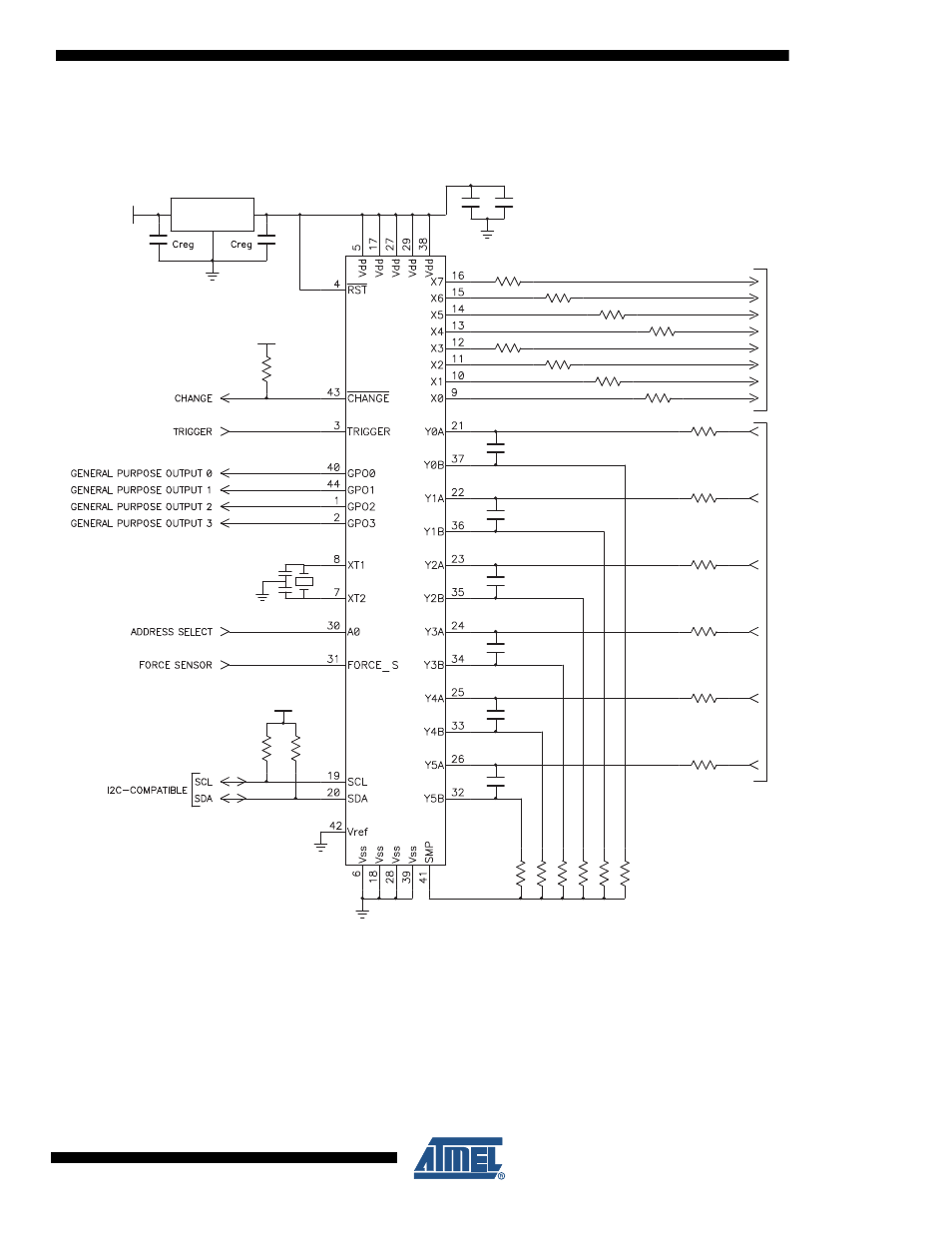
1.3
Schematic
Figure 1-1.
Typical Circuit
Rs3
Rp
Rx4
Rx5
VREG
Rs5 Rs4
Cs5
Cs4
Cs2
Cs1
Rx3
Rs2 Rs1 Rs0
Ry4
Ry1
Rp
Rp
XT1
16MHz
Cs3
Cs0
Rx7
Rx1
Ry5
Ry2
Vunreg
VDD
Ry3
Ry0
MA
TRIX
X
DRIVE
M
A
T
R
IXYS
C
A
N
IN
Rx0
Rx6
VDD
Follow regulator manufacturer's recommended values
for input and output bypass capacitors (Creg).
Rx2
Add two 100nF capacitors: one close to pins 5, 17 and 38,
and another close to pins 27 and 29.
QT5480
NOTES:
1) The central pad on the underside of the MLF chip
is a Vss pin and should be connected to ground.
Do not put any other tracks underneath
the body of the chip.
2) It is important to place all Cs, Rs, Rx and Ry
components physically near to the chip.
3) Leave YnA, YnB unconnected if not used