Detailed description, Pin description – Rainbow Electronics MAX5104 User Manual
Page 6
MAX5104
Low-Power, Dual, Voltage-Output, 12-Bit DAC
with Serial Interface
6
_______________________________________________________________________________________
_______________Detailed Description
The MAX5104 dual, 12-bit, voltage-output DAC is easily
configured with a 3-wire serial interface. The device
includes a 16-bit data-in/data-out shift register, and
each DAC has a double-buffered input composed of an
input register and a DAC register (see
Functional
Diagram). In addition, trimmed internal resistors produce
an internal gain of +2V/V that maximizes output voltage
swing. The amplifier’s offset-adjust pin allows for a DC
shift in the DAC’s output.
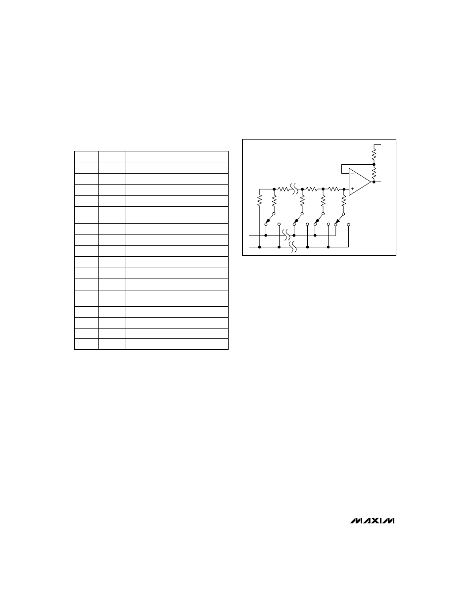
Both DACs use an inverted R-2R ladder network that
produces a weighted voltage proportional to the input
voltage value. Each DAC has its own reference input to
facilitate independent full-scale values. Figure 1 depicts
a simplified circuit diagram of one of the two DACs.
Reference Inputs
The reference inputs accept both AC and DC values
with a voltage range extending from 0 to (V
DD
- 1.4V).
Determine the output voltage using the following equa-
tion (OS_ = AGND):
V
OUT
= (V
REF
·
NB / 4096)
·
2
where NB is the numeric value of the DAC’s binary input
code (0 to 4095) and V
REF
is the reference voltage.
The reference input impedance ranges from 14k
Ω
(1554
hex) to several gigohms (with an input code of 0000
hex). The reference input capacitance is code depen-
dent and typically ranges from 15pF with an input code
of all zeros to 50pF with a full-scale input code.
Output Amplifier
The MAX5104’s output amplifiers have internal resistors
that provide for a gain of +2V/V when OS_ is connected
to AGND. These resistors are trimmed to minimize gain
error. The output amplifiers have a typical slew rate of
0.75V/µs and settle to 1/2LSB within 15µs, with a load
of 10k
Ω
in parallel with 100pF. Loads less than 2k
Ω
degrade performance.
The OS_ pin can be used to produce an adjustable off-
set voltage at the output. For instance, to achieve a 1V
offset, apply -1V to the OS_ pin to produce an output
range from 1V to (1V + V
REF
·
2). Note that the DAC’s
output range is still limited by the maximum output voltage
specification.
Power-Down Mode
The MAX5104 features a software-programmable shut-
down mode that reduces the typical supply current to
2µA. The two DACs can be powered down indepen-
dently, or simultaneously using the appropriate pro-
gramming command. Enter power-down mode by
writing the appropriate input-control word (Table 1). In
power-down mode, the reference inputs and amplifier
outputs become high impedance, and the serial inter-
face remains active. Data in the input registers is saved,
Digital Ground
DGND
9
Serial-Data Output
DOUT
10
User-Programmable Output
UPO
11
Power-Down Lockout. The device can-
not be powered down when
PDL is low.
PDL
12
Reference for DAC B
REFB
13
Active-Low Clear Input. Resets all reg-
isters to zero. DAC outputs go to 0V.
CL
5
Chip-Select Input
CS
6
Serial-Data Input
DIN
7
Serial-Clock Input
SCLK
8
Reference for DAC A
REFA
4
DAC A Offset Adjustment
OSA
3
PIN
DAC A Output Voltage
OUTA
2
Analog Ground
AGND
1
FUNCTION
NAME
14
OSB
DAC B Offset Adjustment
15
OUTB
DAC B Output Voltage
16
V
DD
Positive Power Supply
OUT_
OS_
R
R
D0 D10
D11
D12
2R
2R
2R
2R
2R
R
R
R
REF_
AGND
Figure 1. Simplified DAC Circuit Diagram
_____________________Pin Description