Max5104, Table 3. bipolar code table – Rainbow Electronics MAX5104 User Manual
Page 11
MAX5104
Low-Power, Dual, Voltage-Output, 12-Bit DAC
with Serial Interface
______________________________________________________________________________________
11
MAX5104
V
OUT
= V
REF
[((2
·
NB) / 4096) - 1]
where NB represents the numeric value of the DAC’s
binary input code. Table 3 shows digital codes and the
corresponding output voltage for Figure 11’s circuit.
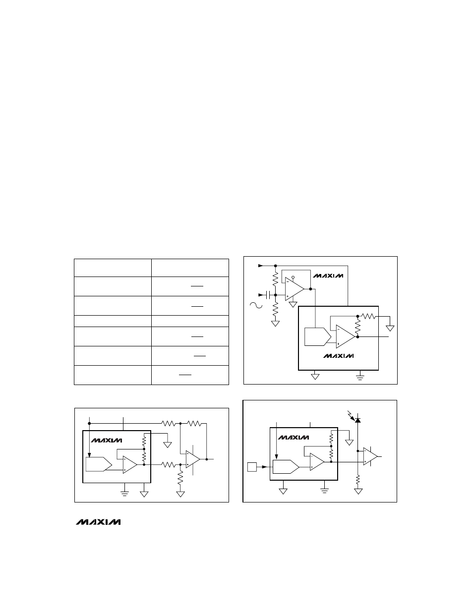
Using an AC Reference
In applications where the reference has an AC signal
component, the MAX5104 has multiplying capabilities
within the reference input voltage range specifications.
Figure 12 shows a technique for applying a sinusoidal
input to REF_, where the AC signal is offset before
being applied to the reference input.
Harmonic Distortion and Noise
The total harmonic distortion plus noise (THD+N) is typ-
ically less than -78dB at full scale with a 1Vp-p input
swing at 5kHz.
Digital Calibration and
Threshold Selection
Figure 13 shows the MAX5104 in a digital calibration
application. With a bright-light value applied to the pho-
todiode (on), the DAC is digitally ramped until it trips
the comparator. The microprocessor (µP) stores this
“high” calibration value. Repeat the process with a dim
light (off) to obtain the dark current calibration.
Table 3. Bipolar Code Table
ANALOG OUTPUT
1 1 1 1 1 1 1 1 1 1 1 1 ( 0 )
1 0 0 0 0 0 0 0 0 0 0 1 ( 0 )
DAC CONTENTS
MSB
LSB
1 0 0 0 0 0 0 0 0 0 0 0 ( 0 )
0V
0 1 1 1 1 1 1 1 1 1 1 1 ( 0 )
0 0 0 0 0 0 0 0 0 0 0 0 ( 0 )
0 0 0 0 0 0 0 0 0 0 0 1 ( 0 )
+V
2047
2048
REF
+V
1
2048
REF
-V
1
2048
REF
+V
2047
4096
REF
⋅
2
-V
2048
2048
- V
REF
REF
=
AGND
DGND
R
R
MAX5104
DAC _
REF_
OS_
OUT_
10k
10k
10k
10k
V-
V+
V
DD
V
OUT
+5V/+3V
Figure 11. Bipolar Output Circuit
DAC_
OUT_
MAX5104
10k
26k
OS_
REF
R
R
V
DD
DGND
AGND
+5V/
+3V
AC
REFERENCE
INPUT
500mVp-p
MAX495
+5V/+3V
Figure 12. AC Reference Input Circuit
AGND
DIN
µ
P
DGND
MAX5104
DAC _
REF_
OS_
OUT_
R
R
V-
V+
PHOTODIODE
V+
V
DD
V
OUT
R
PULLDOWN
+5V/+3V
Figure 13. Digital Calibration
Note:
( ) are for the sub-bit.