Chip information, Pin configuration package information – Rainbow Electronics MAX5104 User Manual
Page 12
Maxim cannot assume responsibility for use of any circuitry other than circuitry entirely embodied in a Maxim product. No circuit patent licenses are
implied. Maxim reserves the right to change the circuitry and specifications without notice at any time.
12
____________________Maxim Integrated Products, 120 San Gabriel Drive, Sunnyvale, CA 94086 408-737-7600
© 1999 Maxim Integrated Products
Printed USA
is a registered trademark of Maxim Integrated Products.
MAX5104
Low-Power, Dual, Voltage-Output, 12-Bit DAC
with Serial Interface
The µP then programs the DAC to set an output voltage
at the midpoint of the two calibrated values. Applications
include tachometers, motion sensing, automatic readers,
and liquid-clarity analysis.
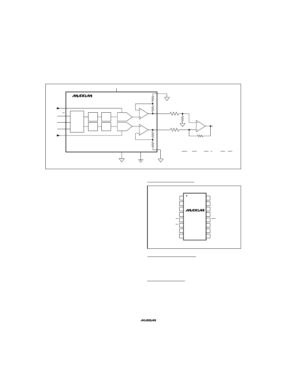
Digital Control of Gain and Offset
The two DACs can be used to control the offset and gain
for curve-fitting nonlinear functions, such as transducer
linearization or analog compression/expansion applica-
tions. The input signal is used as the reference for the
gain-adjust DAC, whose output is summed with the output
from the offset-adjust DAC. The relative weight of each
DAC output is adjusted by R1, R2, R3, and R4 (Figure 14).
Power-Supply Considerations
On power-up, the input and DAC registers clear (set to
zero code). For rated performance, V
REF_
should be at
least 1.4V below V
DD
. Bypass the power supply with a
4.7µF capacitor in parallel with a 0.1µF capacitor to
AGND. Minimize lead lengths to reduce lead inductance.
Grounding and Layout Considerations
Digital and AC transient signals on AGND can create
noise at the output. Connect AGND to the highest quality
ground available. Use proper grounding techniques,
such as a multilayer board with a low-inductance ground
plane. Carefully lay out the traces between channels to
reduce AC cross-coupling and crosstalk. Wire-wrapped
boards and sockets are not recommended. If noise
becomes an issue, shielding may be required.
Chip Information
TRANSISTOR COUNT: 3053
SUBSTRATE CONNECTED TO AGND
AGND
DGND
MAX5104
DACA
V
DD
REFA
V
IN
V
REF
CS
SCLK
DIN
REFB
R1
R3
R
R
R
R
R4
R2
OUTB
OSB
OUTA
OSA
V
OUT
DACB
INPUT
REG A
INPUT
REG B
DAC
REG A
DAC
REG B
– OFFSET
[ ]
V
OUT
=
=
GAIN
[ ]
2NA
4096
NA IS THE NUMERIC VALUE OF THE INPUT CODE FOR DACA.
NB IS THE NUMERIC VALUE OF THE INPUT CODE FOR DACB.
R2
R1+R2
R4
R3
2NB
4096
R4
R3
(
V
IN
)(
)(
1+
) (
V
REF
)( )
[ ] [ ]
SHIFT
REGISTER
Figure 14. Digital Control of Gain and Offset
16
15
14
13
12
11
10
9
1
2
3
4
5
6
7
8
AGND
V
DD
OUTB
OSB
REFB
PDL
UPO
DOUT
DGND
TOP VIEW
MAX5104
QSOP
OUTA
OSA
CS
REFA
CL
DIN
SCLK
Pin Configuration
Package Information
Package information is available on Maxim’s website:
www.maxim-ic.com.