Detailed description, Applications information, Pin description – Rainbow Electronics MAX9034 User Manual
Page 6
MAX9030/MAX9031/MAX9032/MAX9034
Detailed Description
The MAX9030/MAX9031/MAX9032/MAX9034 are sin-
gle/dual/quad low-cost comparators. They have an
operating supply voltage from +2.5V to +5.5V when
operating from a single supply and from ±1.25V to
±2.75V when operating from dual power supplies, and
consume only 35µA. Their common-mode input voltage
range extends from the negative supply to within 1.1V
of the positive supply. Internal hysteresis ensures clean
output switching, even with slow-moving input signals.
Shutdown Mode
The MAX9030 comparator comes with a power-saving
shutdown mode. When in shutdown, the supply current
drops from a typical 35µA to 0.05µA, and the outputs
become high impedance. SHDN has a high input imped-
ance and typically draws 0.1µA when connected to V
SS
or V
DD
. A maximum logic low voltage of 0.3V
✕
V
DD
applied to SHDN places the device in the shutdown
mode. A minimum logic high voltage of 0.7V
✕
V
DD
applied to SHDN will enable normal operation. To dis-
able shutdown, connect SHDN to V
DD
.
Applications Information
Adding Hysteresis
Hysteresis extends the comparator’s noise margin by
increasing the upper threshold and decreasing the
lower threshold. A voltage-divider from the output of the
comparator sets the trip voltage. Therefore, the trip volt-
age is related to the output voltage.
These comparators have 4mV internal hysteresis.
Additional hysteresis can be generated with two resis-
tors using positive feedback (Figure 1). Use the follow-
ing procedure to calculate resistor values:
Low-Cost, Ultra-Small, Single/Dual/Quad
Single-Supply Comparators
6
_______________________________________________________________________________________
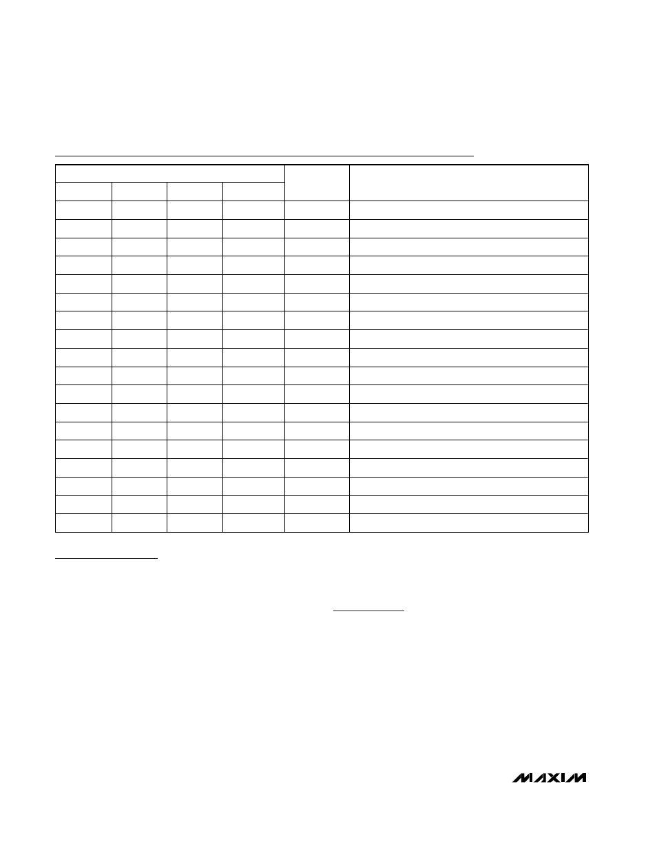
Pin Description
PIN
M A X9 0 3 0 M
A X9 0 3 1 M
A X9 0 3 2 M
A X9 0 3 4
NAME
FUNCTION
1
1
—
—
IN+
Comparator Noninverting Input
2
2
4
11
V
SS
N eg ati ve S up p l y V ol tag e. Byp ass w i th a 0.1µF cap aci tor .
3
3
—
—
IN-
Comparator Inverting Input
4
4
—
—
OUT
Comparator Output
5
—
—
—
SHDN
Shutdown
6
5
8
4
V
DD
P osi ti ve S up p l y V ol tag e. Byp ass w i th a 0.1µF cap aci tor .
—
—
1
1
OUTA
Comparator A Output
—
—
2
2
INA-
Comparator A Inverting Input
—
—
3
3
INA+
Comparator A Noninverting Input
—
—
5
5
INB+
Comparator B Noninverting Input
—
—
6
6
INB-
Comparator B Inverting Input
—
—
7
7
OUTB
Comparator B Output
—
—
—
8
OUTC
Comparator C Output
—
—
—
9
INC-
Comparator C Inverting Input
—
—
—
10
INC+
Comparator C Noninverting Input
—
—
—
12
IND+
Comparator D Noninverting Input
—
—
—
13
IND-
Comparator D Inverting Input
—
—
—
14
OUTD
Comparator D Output