Rainbow Electronics MAX13331 User Manual
Page 2
MAX13330/MAX13331
Automotive DirectDrive Headphone Amplifiers
with Output Protection and Diagnostics
2
_______________________________________________________________________________________
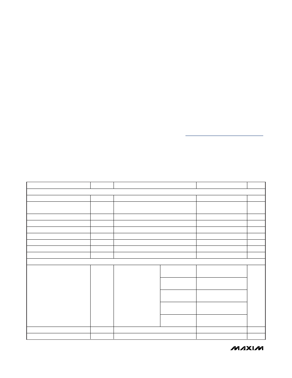
ABSOLUTE MAXIMUM RATINGS
ELECTRICAL CHARACTERISTICS
(V
DD
= V
CPVDD
= +5V, V
SGND
= V
PGND
= 0,
SHDN = V
DD
, C1 = C2 = 1µF, R
L
=
∞, resistive load referenced to ground, for
MAX13330 gain = -1.5V/V (internally set), for MAX13331 gain = -1.5V/V (R
IN
= 30kΩ, R
FB
= 45kΩ), T
A
= T
J
= -40°C to +105°C, unless
otherwise noted. Typical values are at T
A
= +25°C, unless otherwise noted.) (Note 2)
Stresses beyond those listed under “Absolute Maximum Ratings” may cause permanent damage to the device. These are stress ratings only, and functional
operation of the device at these or any other conditions beyond those indicated in the operational sections of the specifications is not implied. Exposure to
absolute maximum rating conditions for extended periods may affect device reliability.
Note 1: Package thermal resistances were obtained using the method described in JEDEC specification JESD51-7, using a four-
layer board. For detailed information on package thermal considerations, refer to
http://www.maxim-ic.com/thermal-tutorial
.
V
DD
, CPVDD to SGND..............................................-0.3V to +6V
V
SS
, CPVSS to SGND ...............................................+0.3V to -6V
V
DD
, CPVDD ............................................................-0.3V to 0.3V
V
SS
, CPVSS..............................................................-0.3V to 0.3V
SHDN, DIAG to SGND................................-0.3V to (V
DD
+ 0.3V)
OUT_ to PGND.......................................(V
CPVSS
- 0.3V) to +45V
IN_ to SGND (MAX13330)................(V
SS
- 0.3V) to (V
DD
+ 0.3V)
IN_ to SGND (MAX13331) ..........................-0.3V to (V
DD
+ 0.3V)
C1P to PGND.........................................-0.3V to (V
CPVDD
+0.3V)
C1N to PGND.............................................(V
SS
- 0.3V) to + 0.3V
Output Short-Circuit Duration.....................................Continuous
Continuous Power Dissipation (T
A
= +70°C)
16-Pin QSOP (derate 8.3mW/°C above +70°C)) ......666.7mW
Junction-to-Case Thermal Resistance (
θ
JC
) (Note 1)
θ
JC
............................................................................... 37°C/W
Junction-to-Ambient Thermal Resistance (
θ
JA
) (Note 1)
θ
JA
............................................................................. 120°C/W
Operating Temperature Range .........................-40°C to +105°C
Junction Temperature ......................................................+150°C
Storage Temperature Range .............................-65°C to +150°C
Lead Temperature (soldering, 10s) .................................+300°C
PARAMETER
SYMBOL
CONDITIONS
MIN
TYP
MAX
UNITS
GENERAL
Amplifier Supply Voltage Range
V
DD
4.0
5.5
V
Charge-Pump Supply Voltage
Range
V
CPVDD
4.0
5.5
V
Charge-Pump Output Voltage
V
CPVSS
-V
DD
V
Quiescent Supply Current
I
DD
R
L
=
∞
10
mA
Shutdown Supply Current
I
SHDN
10
µA
SHDN Input-Logic High
V
IH
2
V
SHDN Input-Logic Low
V
IL
0.8
V
SHDN Input Leakage Current
-1
+1
µA
SHDN to Full Operation Time
t
SON
100
µs
DIAGNOSTICS
No fault
0.02 x
V
DD
OUTR short to
SGND
0.22 x
V
DD
0.25 x
V
DD
0.28 x
V
DD
OUTL short to
SGND
0.47 x
V
DD
0.50 x
V
DD
0.53 x
V
DD
OUTR short to
V
BAT
0.72 x
V
DD
0.75 x
V
DD
0.78 x
V
DD
Diagnostic Output Voltage
V
DIAG
R
DIAG
=
∞,
T
A
= +25°C
OUTL short to
V
BAT
0.97 x
V
DD
V
Short-to-SGND Threshold
130
mA
Short-to-V
BAT
Threshold
130
mA