Component selection – Rainbow Electronics MAX13331 User Manual
Page 11

MAX13330/MAX13331
Automotive DirectDrive Headphone Amplifiers
with Output Protection and Diagnostics
______________________________________________________________________________________
11
Thermal-overload protection limits total power dissipa-
tion in the MAX13330/MAX13331. When the junction
temperature exceeds +145°C (typ), the thermal-protec-
tion circuitry disables the amplifier output stage. The
amplifiers are enabled once the junction temperature
cools by 5°C. This results in a pulsing output under
continuous thermal-overload conditions.
Output Power
The device has been specified for the worst-case sce-
nario, when both inputs are in-phase. Under this condi-
tion, the amplifiers simultaneously draw current from the
charge pump, leading to a proportional reduction in
V
SS
headroom. In typical stereo audio applications, the
left and right signals have differences in both magni-
tude and phase, subsequently leading to an increase in
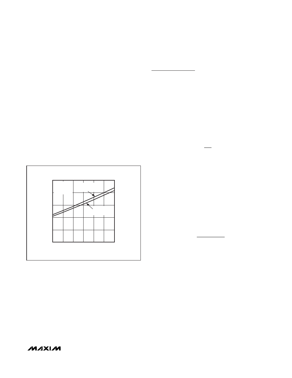
the maximum attainable output power. Figure 4 shows
the two extreme cases for in- and out-of-phase. In reali-
ty, the available power lies between these extremes.
UVLO
The MAX13330/MAX13331 feature a UVLO function that
prevents the device from operating if the supply voltage
is less than 3.6V (typ). This feature ensures proper
operation during brownout conditions and prevents
deep battery discharge. Once the supply voltage
reaches the UVLO threshold, the charge-pump is
turned on and the amplifiers are powered.
Component Selection
Gain-Setting Resistors (MAX13331 Only)
The gain of the MAX13330 is internally set at -1.5V/V.
All gain-setting resistors are integrated into the device,
reducing external component count. The internally set
gain, in combination with DirectDrive, results in a head-
phone amplifier that requires only five tiny 1µF capaci-
tors to complete the amplifier circuit: two for the
charge-pump, two for audio input coupling, and one for
power-supply bypassing (see the
Typical Application
Circuits
). The gain of the MAX13331 amplifier is set
externally as shown in the
Typical Application Circuits
,
the gain is:
Choose feedback resistor values of 10kΩ. Values other
than 10kΩ increase output offset voltage due to the
input bias current, which in turn, increases the amount
of DC current flow to the load.
Input Filtering
The input capacitor (C
IN
), in conjunction with the input
resistor (R
IN
), forms a highpass filter that removes the
DC bias from an incoming signal (see the
Typical
Application Circuits
). The AC-coupling capacitor allows
the device to bias the signal to an optimum DC level.
Assuming zero source impedance, the -3dB point of
the highpass filter is given by:
Choose C
IN
so f
-3dB
is well below the lowest frequency
of interest. For the MAX13330, use the value of R
IN
as
given in the
Electrical Characteristics
table. Setting
f
-3dB
too high affects the device’s low-frequency
response. Use capacitors whose dielectrics have low-
voltage coefficients, such as tantalum or aluminum
electrolytic. Capacitors with high-voltage coefficients,
such as ceramics, can result in increased distortion at
low frequencies.
Charge-Pump Capacitor Selection
Use capacitors with an ESR less than 100mΩ for opti-
mum performance. Low-ESR ceramic capacitors mini-
mize the output resistance of the charge pump. For
best performance over the extended temperature
range, select capacitors with an X7R dielectric.
f
R
C
Hz
dB
IN
IN
−
=
Ч
Ч
3
1
2
π
(
)
A
R
R
V V
V
F
IN
= −
( / )
OUTPUT POWER vs. SUPPLY VOLTAGE
SUPPLY VOLTAGE (V)
OUTPUT POWER (mW)
4.25
5.00
5.25
4.75
4.50
50
100
150
200
250
0
4.00
5.50
f
IN
= 1kHz
R
L
= 32
Ω
THD+N = 10%
INPUTS
IN PHASE
INPUTS 180
°
OUT OF PHASE
Figure 4. Output Power vs. Supply Voltage
