Absolute maximum ratings, Electrical characteristics – Rainbow Electronics MAX6683 User Manual
Page 2
MAX6683
Temperature Sensor and System Monitor
in a 10-Pin µMAX
2
_______________________________________________________________________________________
ABSOLUTE MAXIMUM RATINGS
Stresses beyond those listed under “Absolute Maximum Ratings” may cause permanent damage to the device. These are stress ratings only, and functional
operation of the device at these or any other conditions beyond those indicated in the operational sections of the specifications is not implied. Exposure to
absolute maximum rating conditions for extended periods may affect device reliability.
All Voltages Referenced to GND
All Pins...................................................................-0.3V to +6.0V
SDA, ALERT Current ...........................................-1mA to +50mA
Continuous Power Dissipation (T
A
= +70°C)
10-Pin µMAX (derate 5.6mW/°C above +70°C) ...........444mW
Junction Temperature ......................................................+150°C
Operating Temperature Range .........................-40°C to +125°C
Storage Temperature Range .............................-65°C to +150°C
Lead Temperature (soldering, 10s) .................................+300°C
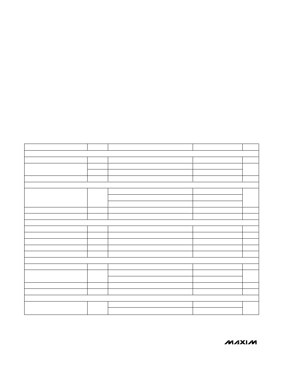
ELECTRICAL CHARACTERISTICS
(T
A
= -40°C to +125°C, unless otherwise noted. Typical values are at V
CC
= +3.3V, T
A
= +25°C.)
PARAMETER
SYMBOL
CONDITIONS
MIN
TYP
MAX
UNITS
POWER SUPPLY
Supply Voltage
V
CC
2.7
5.5
V
I
CC
Operating
200
500
Supply Current
I
SD
Shutdown mode, interface inactive
10
µA
Power-On Reset (POR) Voltage
V
CC
, rising or falling edge
2
V
TEMPERATURE
T
A
= +25°C, V
CC
= +3.3V
±2
-20°C
≤ T
A
≤ +85°C, V
CC
= +3.3V
±3
Accuracy
-40°C
≤ T
A
≤ +125°C, V
CC
= +3.3V
±5
°C
Resolution
Read word mode
0.125
°C
Supply Sensitivity
PSS
0.7
±1.5
°C/V
ADC CHARACTERISTICS
Total Unadjusted Error
TUE
V
IN
> 10LSBs
±1.5
%
Differential Nonlinearity
DNL
V
IN
> 10LSBs
±1
LSB
Supply Sensitivity
PSS
±1
LSB/V
Input Resistance
R
IN
1.8V
IN
, 2.5V
IN
, 5V
IN
100
150
200
k
Ω
Total Monitoring Cycle Time
t
c
(Note 1)
200
300
ms
SCL, SDA, ADD
Logic Input Low Voltage
V
IL
0.8
V
V
CC
≤ 3.6V
2.0
Logic Input High Voltage
V
IH
V
CC
> 3.6V
2.6
V
Input Leakage Current
I
LEAK
V
IN
= 0 or 5V
±1
µA
Output Low Voltage
V
OL
I
SINK
= 3mA
400
mV
ALERT
I
SINK
= 1.2mA, V
CC
> 2.7V
0.3
Output Low Voltage
V
OLA
I
SINK
= 3.2mA, V
CC
> 4.5V
0.4
V