Max6683 – Rainbow Electronics MAX6683 User Manual
Page 12

MAX6683
The MAX6683 also responds to the SMBus alert
response address (see Alert Response Address).
Alert Response Address
The SMBus alert response interrupt pointer provides
quick fault identification for simple slave devices that
lack the complex, expensive logic needed to be a bus
master. Usually the ALERT outputs of several slave
devices are wire-ORed to the same interrupt input of
the host master. Upon receiving an interrupt signal, the
host master can broadcast a receive byte transmission
(Figure 2) with the alert response address (0001 100).
A read operation is denoted by a 1 in the eighth
address bit. Then, any slave device that generated an
interrupt attempts to identify itself by putting its own
address on the bus.
The alert response can activate several different slave
devices simultaneously, similar to the I
2
C general call. If
more than one slave attempts to respond, bus arbitra-
tion rules apply, and the device with the lower address
code wins. The losing device does not generate an
acknowledge signal and continues to hold the interrupt
line low until serviced. The MAX6683 does not automat-
ically clear its ALERT when it responds to an alert
response address. The host master must then clear or
mask the ALERT by reading the Interrupt Status
Register, writing to the Interrupt Mask Register, or set-
ting bit 1 of the Configuration Register to zero before it
can identify other slaves generating an interrupt.
Command Byte Functions
The 8-bit Command Byte Register (Table 1) is the mas-
ter index that points to the other data, configuration,
limits, and address registers within the MAX6683. The
functions of those other registers are described below.
Configuration Byte Functions
The Configuration Register (Table 4) is a read-write reg-
ister with several functions:
•
Bit 0 puts the MAX6683 into software standby mode
(STOP) or autoconvert (START) mode. The 2-wire
interface is still active in the standby mode. All volt-
age and temperature limits should be set before
setting this bit to 1.
•
Bit 1 enables and disables the ALERT output.
Setting this bit to 1 enables the ALERT output.
•
Bit 2 is reserved.
•
Bit 3 clears the ALERT output and stops the moni-
toring loop when set to 1. Clearing the output does
not affect the contents of the Interrupt Status
Registers.
•
Bit 4 sets the analog-to-digital conversion speed to
minimize interference from power-line frequencies.
Setting this bit to 1 can improve accuracy when the
power-line frequency is 50Hz. When the power-line
frequency is 60Hz, bit 4 should be zero.
•
Bit 5 reduces the oversampling ratio in the ADC
from 8 to 2. This reduces the monitoring cycle time
by a factor of 4 to typically 50ms at the cost of
reduced noise rejection.
•
Bit 6 is reserved.
•
Bit 7 resets all register values to their power-up
default values. To reset all registers, set bit 7 to 1.
This also resets bit 7 to its power-up value of zero.
Read Temperature
The MAX6683 reads out temperature in an 8-, 9-, or 11-bit
two's complement format. To obtain the 8-bit temperature
data (7 bits plus sign), execute a Read Byte command to
the Temperature Data Register (address 27h).
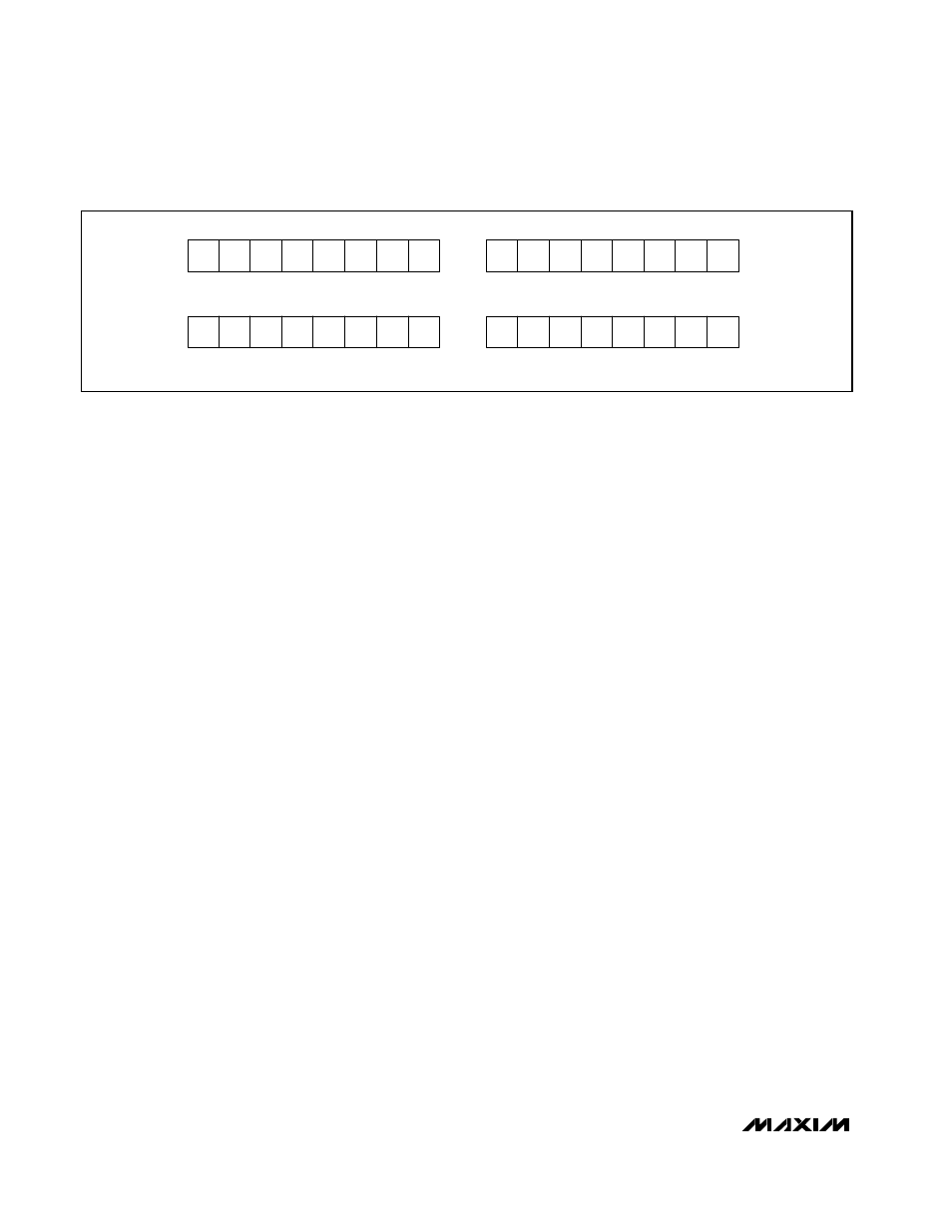
To obtain the 11-bit temperature data (10 bits plus
sign), execute a Read Word command to the
Temperature Data Register (address 27h). When per-
forming a Read Word operation, the MAX6683 writes
the 11 bits of data to the bus in two 8-bit words. The
Temperature Sensor and System Monitor
in a 10-Pin µMAX
12
______________________________________________________________________________________
D2
D1
D0
X
X
X
X
X
X
X
X
X
X
X
X
LOWER BYTE
D10
D9
D8
D7
D6
D5
D4
UPPER BYTE
D3
11-BIT READ FORMAT
D0
LOWER BYTE
D8
D7
D6
D5
D4
D3
D2
UPPER BYTE
D1
9-BIT READ FORMAT
X = DON'T CARE
Figure 5. Read Temperature Format
