Smbus/i, C-compatible digital interface, Slave address – Rainbow Electronics MAX6683 User Manual
Page 11

rupt continues to be generated on subsequent mea-
surements until the temperature falls below T
HOT
.
SMBus/I
2
C-Compatible Digital Interface
From a software prospective, the MAX6683 appears as a
set of byte-wide registers that contain voltage and tem-
perature data, alarm threshold values, or control bits.
The device employs five standard SMBus protocols:
write byte, read byte, read word, send byte, and
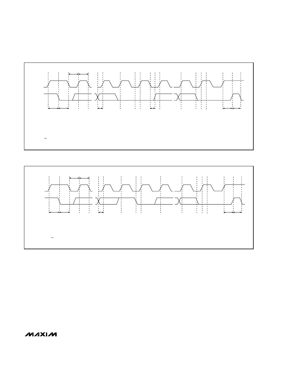
receive byte (Figures 2, 3, 4).
Slave Address
The device address can be set to one of four different
values by pin strapping ADD to GND, SDA, SCL, or
V
CC
, so more than one MAX6683 can reside on the
same bus without address conflicts (Table 1). The
address pin state is checked at the beginning of each
SMBus/I
2
C transaction and is insensitive to glitches on
V
CC
. Any address code can also be written to the Serial
Address Register and overwrites the code set by con-
necting the ADD pin until the MAX6683 is taken through
a POR cycle.
MAX6683
Temperature Sensor and System Monitor
in a 10-Pin µMAX
______________________________________________________________________________________
11
SMBCLK
A
B
C
D
E
F
G
H
I
J
K
SMBDATA
t
SU:STA
t
HD:STA
t
LOW
t
HIGH
t
SU:DAT
t
HD:DAT
t
SU:STO
t
BUF
A = START CONDITION
B = MSB OF ADDRESS CLOCKED INTO SLAVE
C = LSB OF ADDRESS CLOCKED INTO SLAVE
D = R/W BIT CLOCKED INTO SLAVE
E = SLAVE PULLS SMBDATA LINE LOW
L
M
F = ACKNOWLEDGE BIT CLOCKED INTO MASTER
G = MSB OF DATA CLOCKED INTO SLAVE
H = LSB OF DATA CLOCKED INTO SLAVE
I = SLAVE PULLS SMBDATA LINE LOW
J = ACKNOWLEDGE CLOCKED INTO MASTER
K = ACKNOWLEDGE CLOCK PULSE
L = STOP CONDITION, DATA EXECUTED BY SLAVE
M = NEW START CONDITION
Figure 3. SMBus Write Timing Diagram
SMBCLK
A
B
C
D
E
F
G
H
I
J
K
SMBDATA
t
SU:STA
t
HD:STA
t
LOW
t
HIGH
t
SU:DAT
t
SU:STO
t
BUF
L
M
E = SLAVE PULLS SMBDATA LINE LOW
F = ACKNOWLEDGE BIT CLOCKED INTO MASTER
G = MSB OF DATA CLOCKED INTO MASTER
H = LSB OF DATA CLOCKED INTO MASTER
I = MASTER PULLS DATA LINE LOW
J = ACKNOWLEDGE CLOCKED INTO SLAVE
K = ACKNOWLEDGE CLOCK PULSE
L = STOP CONDITION
M = NEW START CONDITION
A = START CONDITION
B = MSB OF ADDRESS CLOCKED INTO SLAVE
C = LSB OF ADDRESS CLOCKED INTO SLAVE
D = R/W BIT CLOCKED INTO SLAVE
Figure 4. SMBus Read Timing Diagram
