Pin description pin configuration – Rainbow Electronics MAX15058 User Manual
Page 9
High-Efficiency, 3A, Current-Mode
Synchronous, Step-Down Switching Regulator
MAX15058
_______________________________________________________________________________________ 9
Pin Description
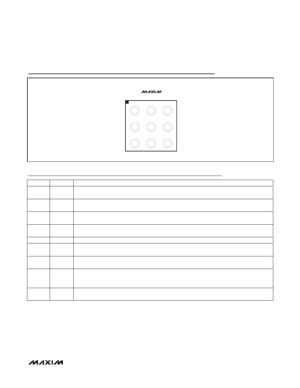
Pin Configuration
BUMP
NAME
FUNCTION
A1
GND
Analog Ground/Low-Side Switch Source Terminal. Connect to the PCB copper plane at one point near
the input bypass capacitor return terminal.
A2
LX
Inductor Connection. Connect LX to the switched side of the inductor. LX is high impedance when the
IC is in shutdown mode.
A3
IN
Input Power Supply. Input supply range is from 2.7V to 5.5V. Bypass with a minimum 10FF ceramic
capacitor to GND. See Figures 5 and 6.
B1
COMP
Voltage Error-Amplifier Output. Connect the necessary compensation network from COMP to GND. See
the Closing the Loop: Designing the Compensation Circuitry section.
B2
SKIP
Skip-Mode Input. Connect to EN to select skip mode or leave unconnected for normal operation.
B3
EN
Enable Input. EN is a digital input that turns the regulator on and off. Drive EN high to turn on the regula-
tor. Connect to IN for always-on operation.
C1
FB
Feedback Input. Connect FB to the center tap of an external resistor-divider from the output to GND to
set the output voltage from 0.6V up to 94% of V
IN
.
C2
SS/REFIN
Soft-Start/External Voltage Reference Input. Connect a capacitor from SS/REFIN to GND to set the startup
time. See the Setting the Soft-Start Time section for details on setting the soft-start time. Apply a voltage
reference from 0V to V
IN
- 1.5V to drive soft-start externally.
C3
PGOOD
Open-Drain Power-Good Output. PGOOD goes high when FB is above 555mV and pulls low if FB is
below 527mV.
WLP
TOP VIEW
(BUMPS ON BOTTOM)
SS/REFIN
FB
PGOOD
SKIP
COMP
EN
LX
GND
IN
MAX15058
A1
B1
C1
C2
C3
B2
B3
A3
A2