Rainbow Electronics MAX15058 User Manual
Page 19

High-Efficiency, 3A, Current-Mode
Synchronous, Step-Down Switching Regulator
MAX15058
______________________________________________________________________________________ 19
Power Dissipation
The MAX15058 is available in a 9-bump WLP package
and can dissipate up to 1127mW at T
A
= +70NC. When
the die temperature exceeds +150NC, the thermal-shut-
down protection is activated (see the Thermal-Shutdown
Protection section).
Layout Procedure
Careful PCB layout is critical to achieve clean and stable
operation. It is highly recommended to duplicate the
MAX15058 Evaluation Kit layout for optimum perfor-
mance. If deviation is necessary, follow these guidelines
for good PCB layout:
1) Connect the signal and ground planes at a single point
immediately adjacent to the GND bump of the IC.
2) Place capacitors on IN and SS/REFIN as close as
possible to the IC and the corresponding pad using
direct traces.
3) Keep the high-current paths as short and wide as
possible. Keep the path of switching current short
and minimize the loop area formed by LX, the output
capacitors, and the input capacitors.
4) Connect IN, LX, and GND separately to a large cop-
per area to help cool the IC to further improve effi-
ciency.
5) Ensure all feedback connections are short and
direct. Place the feedback resistors and compensa-
tion components as close as possible to the IC.
6) Route high-speed switching nodes (such as LX)
away from sensitive analog areas (such as FB and
COMP).
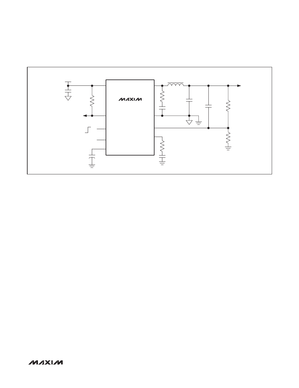
Figure 5. Application Circuit for PWM Mode Operation
LX
GND
FB
COMP
C
OUT
22µF x 2
OUTPUT
1.8V AT 3A
R
2
4.02kI
R
1
8.06kI
R
C
5.36kI
C
C
1nF
L
OUT
1µH
C
FF
100pF
1.2I
1nF
R
PULL
20kI
C
IN
22µF
IN
PGOOD
EN
ENABLE
SKIP
ON
OFF
C
SS
22nF
SS/REFIN
MAX15058
INPUT
2.8V TO 5.5V
(ICE IN06142)
