Rainbow Electronics MAX15058 User Manual
Page 13
High-Efficiency, 3A, Current-Mode
Synchronous, Step-Down Switching Regulator
MAX15058
______________________________________________________________________________________ 13
set to 0.3). In addition, the peak inductor current, I
L_PK
,
must always be below the minimum high-side current-
limit value, I
HSCL
, and the inductor saturation current
rating, I
L_SAT
.
Ensure that the following relationship is satisfied:
(
)
L_PK
LOAD
L
HSCL_, L_SAT
1
I
I
I
min I
I
2
=
+ ∆ <
Input Capacitor Selection
The input capacitor reduces the peak current drawn from
the input power supply and reduces switching noise in
the device. The total input capacitance must be equal to
or greater than the value given by the following equation
to keep the input ripple voltage within the specification
and minimize the high-frequency ripple current being fed
back to the input source:
LOAD
OUT
IN
SW
IN_RIPPLE
IN
I
V
C
f
V
V
=
Ч
Ч ∆
where DV
IN_RIPPLE
is the maximum-allowed input ripple
voltage across the input capacitors and is recommend-
ed to be less than 2% of the minimum input voltage,
f
SW
is the switching frequency (1MHz), and I
LOAD
is the
output load. The impedance of the input capacitor at
the switching frequency should be less than that of the
input source so high-frequency switching currents do not
pass through the input source, but are instead shunted
through the input capacitor.
The input capacitor must meet the ripple current require-
ment imposed by the switching currents. The RMS input
ripple current is given by:
(
)
OUT
IN
OUT
RIPPLE
LOAD
IN
V
V
V
I
I
V
×
−
=
where I
RIPPLE
is the input RMS ripple current.
Output Capacitor Selection
The key selection parameters for the output capacitor
are capacitance, ESR, ESL, and voltage rating. The
parameters affect the overall stability, output ripple volt-
age, and transient response of the DC-DC converter.
The output ripple occurs due to variations in the charge
stored in the output capacitor, the voltage drop due to
the capacitor’s ESR, and the voltage drop due to the
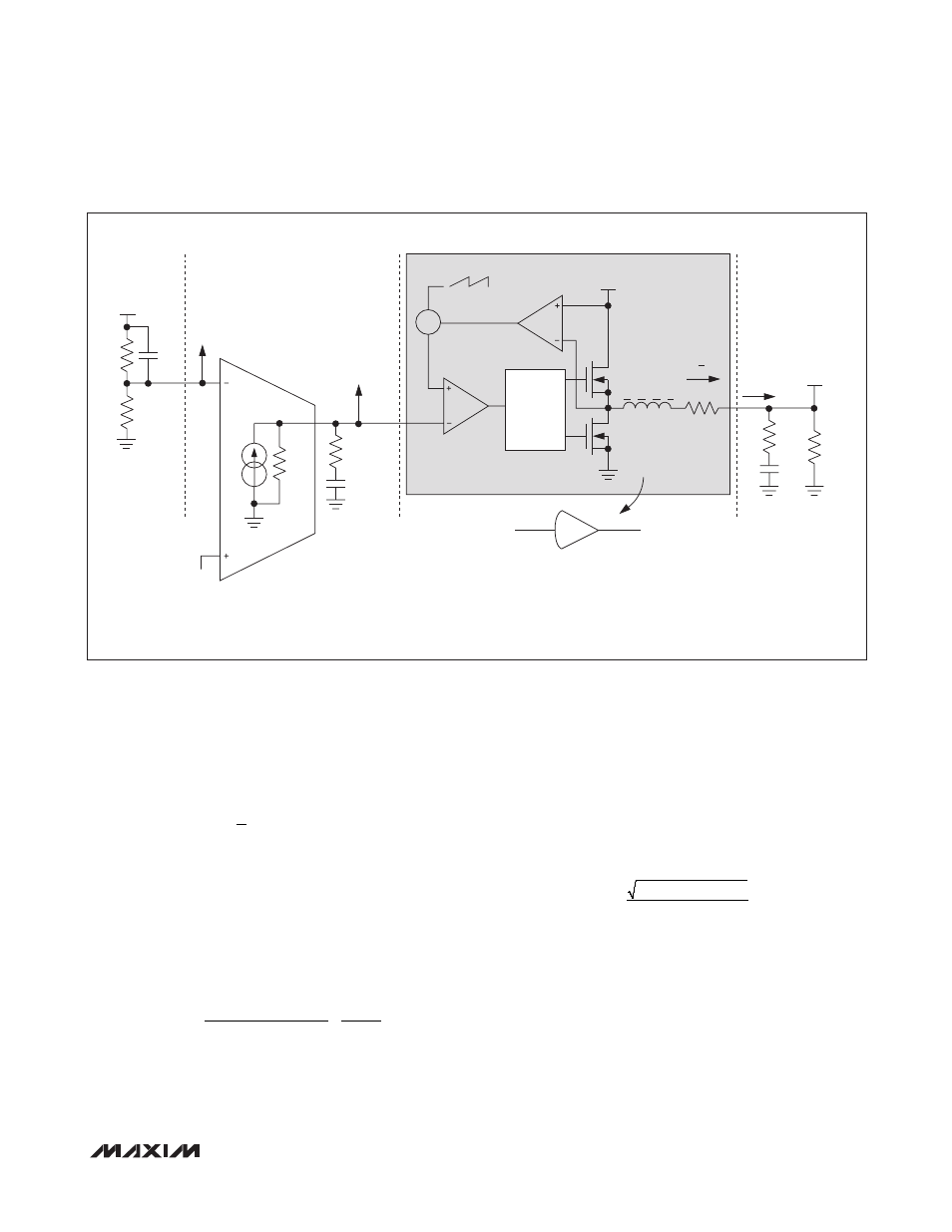
Figure 1. Peak Current-Mode Regulator Transfer Model
L
V
COMP
I
OUT
COMPARATOR
COMP
V
COMP
V
FB
R
C
R
OUT
g
MV
V
IN
POWER MODULATOR
OUTPUT FILTER
AND LOAD
NOTE: THE G
MOD
STAGE SHOWN ABOVE MODELS THE AVERAGE CURRENT OF
THE INDUCTOR, I
L
, INJECTED INTO THE OUTPUT LOAD, I
OUT
, e.g., I
L
= I
OUT
.
THIS CAN BE USED TO SIMPLIFY/MODEL THE MODULATION/CONTROL/POWER
STATE CIRCUITRY SHOWN WITHIN THE BOXED AREA.
*NOTE: C
FF
IS OPTIONAL AND DESIGNED TO EXTEND THE
REGULATOR’S GAIN BANDWIDTH AND INCREASED PHASE
MARGIN FOR SOME LOW-DUTY CYCLE APPLICATIONS.
ERROR AMPLIFIER
FEEDBACK
DIVIDER
SLOPE
COMPENSATION
RAMP
g
MC
DCR
I
L
Q
LS
V
OUT
V
OUT
Q
HS
I
OUT
ESR
C
OUT
R
LOAD
C
C
REF
R
OUT
= 10
AVEA(dB)/20
/g
MV
*C
FF
FB
R1
R2
G
MOD
PWM
CONTROL
LOGIC
C