Functional description – Rainbow Electronics АDC0805 User Manual
Page 23
Functional Description
(Continued)
4 2 Interfacing the Z-80
The Z-80 control bus is slightly different from that of the
8080 General RD and WR strobes are provided and sepa-
rate memory request MREQ and I O request IORQ sig-
nals are used which have to be combined with the general-
ized strobes to provide the equivalent 8080 signals An ad-
vantage of operating the A D in I O space with the Z-80 is
that the CPU will automatically insert one wait state (the RD
and WR strobes are extended one clock period) to allow
more time for the I O devices to respond Logic to map the
A D in I O space is shown in
Figure 13
TL H 5671 – 23
FIGURE 13 Mapping the A D as an I O Device
for Use with the Z-80 CPU
Additional I O advantages exist as software DMA routines
are available and use can be made of the output data trans-
fer which exists on the upper 8 address lines (A8 to A15)
during I O input instructions For example MUX channel
selection for the A D can be accomplished with this operat-
ing mode
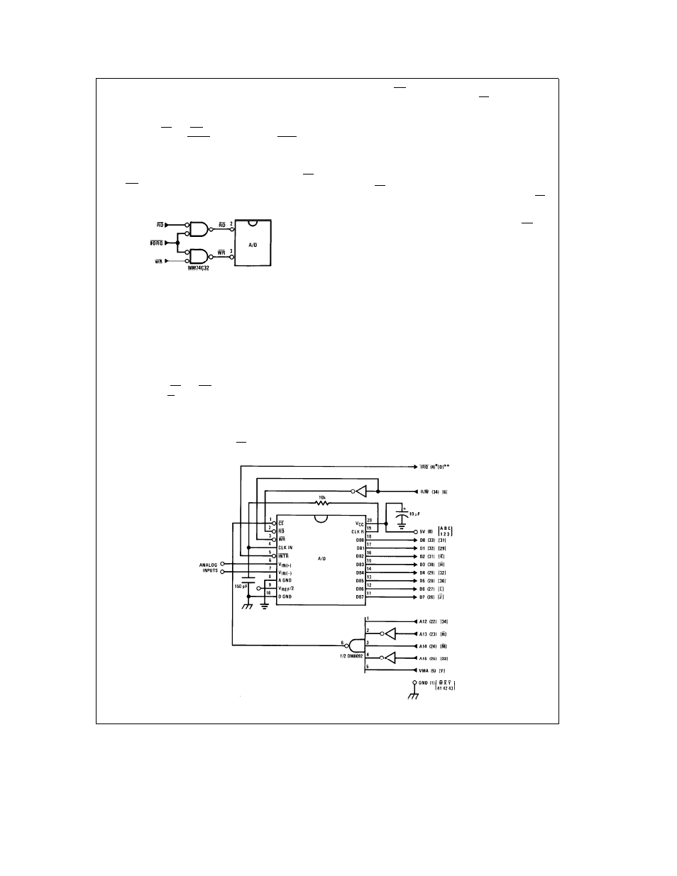
4 3 Interfacing 6800 Microprocessor Derivatives
(6502 etc )
The control bus for the 6800 microprocessor derivatives
does not use the RD and WR strobe signals Instead it em-
ploys a single R W line and additional timing if needed can
be derived fom the w2 clock All I O devices are memory
mapped in the 6800 system and a special signal VMA
indicates that the current address is valid
Figure 14
shows
an interface schematic where the A D is memory mapped in
the 6800 system For simplicity the CS decoding is shown
using
DM8092 Note that in many 6800 systems an al-
ready decoded 4 5 line is brought out to the common bus at
pin 21 This can be tied directly to the CS pin of the A D
provided that no other devices are addressed at HX ADDR
4XXX or 5XXX
The following subroutine performs essentially the same
function as in the case of the 8080A interface and it can be
called from anywhere in the user’s program
In
Figure 15
the ADC0801 series is interfaced to the M6800
microprocessor through (the arbitrarily chosen) Port B of the
MC6820 or MC6821 Peripheral Interface Adapter (PIA)
Here the CS pin of the A D is grounded since the PIA is
already memory mapped in the M6800 system and no CS
decoding is necessary Also notice that the A D output data
lines are connected to the microprocessor bus under pro-
gram control through the PIA and therefore the A D RD pin
can be grounded
A sample interface program equivalent to the previous one
is shown below
Figure 15
The PIA Data and Control Regis-
ters of Port B are located at HEX addresses 8006 and 8007
respectively
5 0 GENERAL APPLICATIONS
The following applications show some interesting uses for
the A D The fact that one particular microprocessor is used
is not meant to be restrictive Each of these application cir-
cuits would have its counterpart using any microprocessor
that is desired
5 1 Multiple ADC0801 Series to MC6800 CPU Interface
To transfer analog data from several channels to a single
microprocessor system a multiple converter scheme pre-
sents several advantages over the conventional multiplexer
single-converter approach With the ADC0801 series the
differential inputs allow individual span adjustment for each
channel Furthermore all analog input channels are sensed
simultaneously which essentially divides the microproces-
sor’s total system servicing time by the number of channels
since all conversions occur simultaneously This scheme is
shown in
Figure 16
TL H 5671 – 24
Note 1
Numbers in parentheses refer to MC6800 CPU pin out
FIGURE 14 ADC0801-MC6800 CPU Interface
Note 2
Number or letters in brackets refer to standard M6800 system common bus code
23