Functional description – Rainbow Electronics АDC0805 User Manual
Page 13
Functional Description
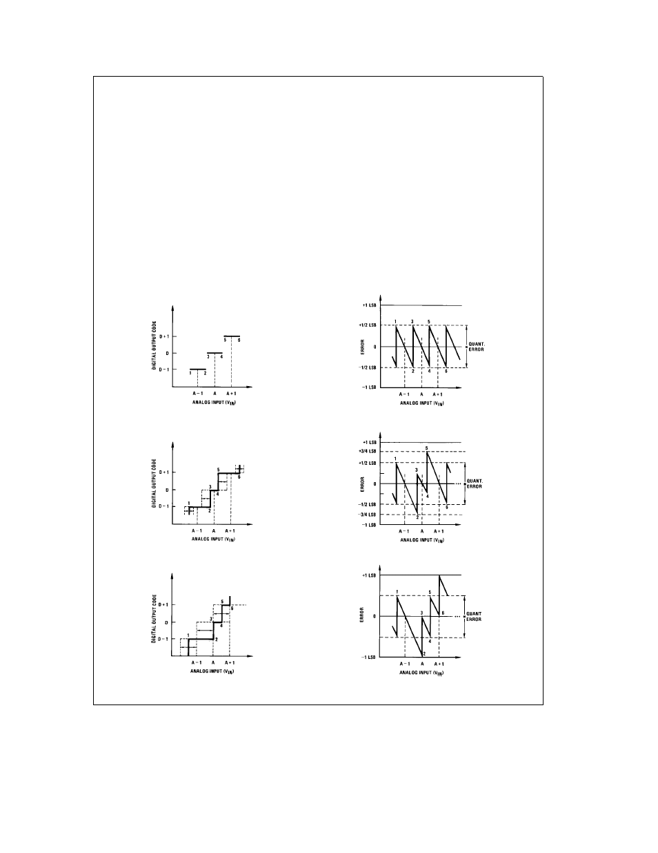
1 0 UNDERSTANDING A D ERROR SPECS
A perfect A D transfer characteristic (staircase waveform) is
shown in
Figure 1a
The horizontal scale is analog input
voltage and the particular points labeled are in steps of 1
LSB (19 53 mV with 2 5V tied to the V
REF
2 pin) The digital
output codes that correspond to these inputs are shown as
Db1 D and Da1 For the perfect A D not only will center-
value (Ab1 A Aa1
) analog inputs produce the cor-
rect output ditigal codes but also each riser (the transitions
between adjacent output codes) will be located
g
LSB
away from each center-value As shown the risers are ideal
and have no width Correct digital output codes will be pro-
vided for a range of analog input voltages that extend
g
LSB from the ideal center-values Each tread (the range of
analog input voltage that provides the same digital output
code) is therefore 1 LSB wide
Figure 1b
shows a worst case error plot for the ADC0801
All center-valued inputs are guaranteed to produce the cor-
rect output codes and the adjacent risers are guaranteed to
be no closer to the center-value points than
g
LSB In
other words if we apply an analog input equal to the center-
value
g
LSB
we guarantee
that the A D will produce the
correct digital code The maximum range of the position of
the code transition is indicated by the horizontal arrow and it
is guaranteed to be no more than
LSB
The error curve of
Figure 1c
shows a worst case error plot
for the ADC0802 Here we guarantee that if we apply an
analog input equal to the LSB analog voltage center-value
the A D will produce the correct digital code
Next to each transfer function is shown the corresponding
error plot Many people may be more familiar with error plots
than transfer functions The analog input voltage to the A D
is provided by either a linear ramp or by the discrete output
steps of a high resolution DAC Notice that the error is con-
tinuously displayed and includes the quantization uncertain-
ty of the A D For example the error at point 1 of
Figure 1a
is a
LSB because the digital code appeared
LSB in
advance of the center-value of the tread The error plots
always have a constant negative slope and the abrupt up-
side steps are always 1 LSB in magnitude
Transfer Function
Error Plot
a) Accuracye
g
0 LSB A Perfect A D
Transfer Function
Error Plot
b) Accuracye
g
LSB
Transfer Function
Error Plot
c) Accuracye
g
LSB
TL H 5671 – 12
FIGURE 1 Clarifying the Error Specs of an A D Converter
13