Functional description – Rainbow Electronics АDC0805 User Manual
Page 15
Functional Description
(Continued)
After the ‘‘1’’ is clocked through the 8-bit shift register
(which completes the SAR search) it appears as the input to
the D-type latch LATCH 1 As soon as this ‘‘1’’ is output
from the shift register the AND gate G2 causes the new
digital word to transfer to the TRI-STATE output latches
When LATCH 1 is subsequently enabled the Q output
makes a high-to-low transition which causes the INTR F F
to set An inverting buffer then supplies the INTR input sig-
nal
Note that this SET control of the INTR F F remains low for
8 of the external clock periods (as the internal clocks run at
of the frequency of the external clock) If the data output
is continuously enabled (CS and RD both held low) the
INTR output will still signal the end of conversion (by a high-
to-low transition) because the SET input can control the Q
output of the INTR F F even though the RESET input is
constantly at a ‘‘1’’ level in this operating mode This INTR
output will therefore stay low for the duration of the SET
signal which is 8 periods of the external clock frequency
(assuming the A D is not started during this interval)
When operating in the free-running or continuous conver-
sion mode (INTR pin tied to WR and CS wired low
see
also section 2 8) the START F F is SET by the high-to-low
transition of the INTR signal This resets the SHIFT REGIS-
TER which causes the input to the D-type latch LATCH 1
to go low As the latch enable input is still present the Q
output will go high which then allows the INTR F F to be
RESET This reduces the width of the resulting INTR output
pulse to only a few propagation delays (approximately 300
ns)
When data is to be read the combination of both CS and
RD being low will cause the INTR F F to be reset and the
TRI-STATE output latches will be enabled to provide the 8-
bit digital outputs
2 1 Digital Control Inputs
The digital control inputs (CS RD and WR) meet standard
T
2
L logic voltage levels These signals have been renamed
when compared to the standard A D Start and Output En-
able labels In addition these inputs are active low to allow
an easy interface to microprocessor control busses For
non-microprocessor based applications the CS input (pin 1)
can be grounded and the standard A D Start function is
obtained by an active low pulse applied at the WR input (pin
3) and the Output Enable function is caused by an active
low pulse at the RD input (pin 2)
2 2 Analog Differential Voltage Inputs and
Common-Mode Rejection
This A D has additional applications flexibility due to the
analog differential voltage input The V
IN
(b) input (pin 7)
can be used to automatically subtract a fixed voltage value
from the input reading (tare correction) This is also useful in
4 mA – 20 mA current loop conversion In addition common-
mode noise can be reduced by use of the differential input
The time interval between sampling V
IN
(a) and V
IN
(b) is 4-
clock periods The maximum error voltage due to this
slight time difference between the input voltage samples is
given by
D
V
e
(MAX) e (V
P
) (2
q
f
cm
)
4 5
f
CLK
J
where
D
V
e
is the error voltage due to sampling delay
V
P
is the peak value of the common-mode voltage
f
cm
is the common-mode frequency
As an example to keep this error to
LSB (E5 mV) when
operating with a 60 Hz common-mode frequency f
cm
and
using a 640 kHz A D clock f
CLK
would allow a peak value
of the common-mode voltage V
P
which is given by
V
P
e
D
V
e(MAX)
(f
CLK
)
(2
q
f
cm
) (4 5)
or
V
P
e
(5
c
10
b
3
) (640
c
10
3
)
(6 28) (60) (4 5)
which gives
V
P
j
1 9V
The allowed range of analog input voltages usually places
more severe restrictions on input common-mode noise lev-
els
An analog input voltage with a reduced span and a relatively
large zero offset can be handled easily by making use of the
differential input (see section 2 4 Reference Voltage)
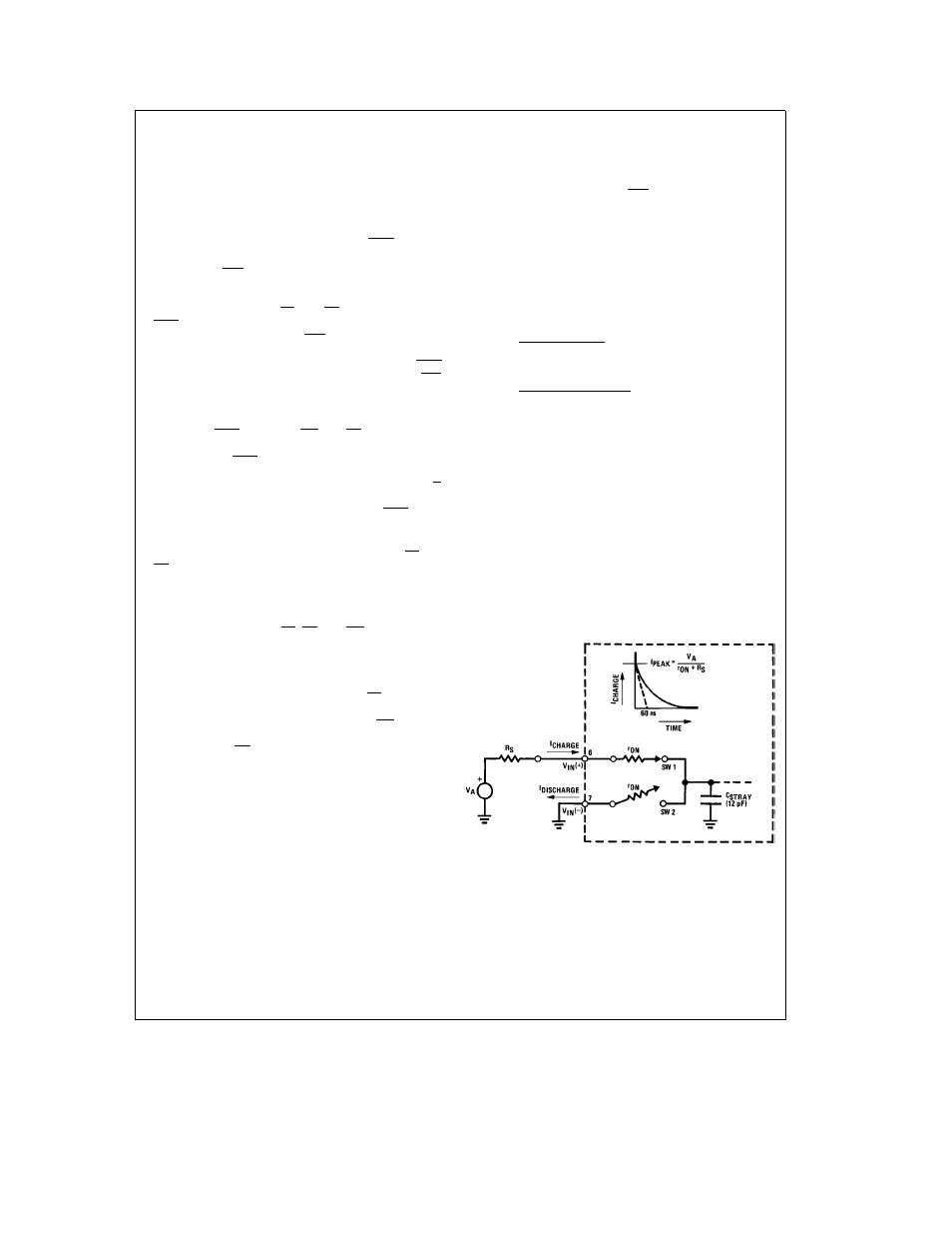
2 3 Analog Inputs
2 3 1 Input Current
Normal Mode
Due to the internal switching action displacement currents
will flow at the analog inputs This is due to on-chip stray
capacitance to ground as shown in
Figure 3
TL H 5671 – 14
r
ON
of SW 1 and SW 2 j 5 kX
r
e
r
ON
C
STRAY
j
5 kX
c
12 pF
e
60 ns
FIGURE 3 Analog Input Impedance
15